Method and apparatus transporting charges in semiconductor device and semiconductor memory device

a semiconductor and memory device technology, applied in semiconductor devices, radio frequency controlled devices, instruments, etc., can solve the problems of poor injection efficiency, high voltage to support memory operation, and all the above mechanisms and attempts

Inactive Publication Date: 2006-01-05
MARVELL ASIA PTE LTD
View PDF99 Cites 30 Cited by
  • Summary
  • Abstract
  • Description
  • Claims
  • Application Information

AI Technical Summary

Problems solved by technology

All the above mechanisms and attempts, however, have poor injection efficiency (defined as the ratio of number of carriers collected to the number of carriers supplied).
Further, these mechanisms require high voltages to support the memory operation, and voltage as high as 10V is often seen.
It is believed that the high voltage demands stringent control on the quality of the insulator surrounding the floating gate.
The memories operated under these mechanisms thus are vulnerable to manufacturing and reliability problems.

Method used


Image

  • Method and apparatus transporting charges in semiconductor device and semiconductor memory device
  • Method and apparatus transporting charges in semiconductor device and semiconductor memory device
  • Method and apparatus transporting charges in semiconductor device and semiconductor memory device

Examples


embodiment 100

[0160] Embodiment 100

[0161]FIG. 22 shows a cross-sectional view of cell architecture 100 in accordance with one embodiment on cell structure of the present invention. Referring to cell 100 of FIG. 22, there is shown a conductor-filter system 59 of the type described in connection with FIGS. 7, 9, 11 and 13, a conductor-insulator system 60 of the type described in connection with FIGS. 1, 5 and 6, a charge storage region (“CSR”) 66 in the form of a floating gate (“FG”) 66100, and a channel dielectric (“CD”) 68. The conductor-filter system 59 comprises a tunneling-gate (“TG”) 61, and a filter 52, wherein TG 61 corresponds to the conductor of the system 59. The filter 52 provides the band-pass filtering function as described in connection with FIG. 7, the charge-filtering function as described in connection with FIGS. 10, 12A, 13 and 14, the voltage divider function as described in connection with FIG. 12B, and the mass-filtering function as described in connection with FIG. 15. In a p...

embodiment 200

[0169] Embodiment 200

[0170] Turning now to FIG. 23, a slight variation of the cell 100 of FIG. 22 is presented in a memory cell 200. The cell 200 is in all respect except one the same as cell 100 of FIG. 22. The difference is that instead of a conductive region of FG 66100 as CSR 66, the cell 200 is provided with a plurality of spaced-apart nano-particles 66200 formed in nanometer scale as CSR 66. The nano-particles 66200 is typically in an oval shape having a dimension in the range of about 2 nm to about 10 nm, and is shown contacting CD 68 and formed in RD 64. The RD 64 is shown in a single layer and can be a layer of a stack of different dielectrics, such as a layer of oxide / nitride / oxide stack. The nano-particles as the storage sites can be silicon nano-crystals each in an oval shape having a diameter in the range of about 2 nm to about 7 nm, and can be formed by using well-known CVD technique. The nano-particles can be other types of semiconductor materials (e.g. Ge, SiGe alloy...

embodiment 300

[0172] Embodiment 300

[0173]FIG. 24 provides cross sectional view on a memory cell 300 of another embodiment in accordance with the present invention. The cell 300 is in all respect except one the same as cell 100 of FIG. 22. The difference is that instead of a conductive region for CSR 66, the cell 300 provides a CSR 66 of trapping dielectric having a plurality of trapping centers (traps 66300). The dielectric CSR 66 uses traps 66300 as the charge storage sites and can be a nitride layer formed, for example, by using LPCVD (Low-Pressure-Chemical-Vapor-Deposition) technique well-known in the art. Other dielectrics such as HfO2 and ZrO2 having traps of a deeper trapping energy can also be considered as material for the trapping dielectric.

[0174] Both cells 200 and 300 utilize scheme storing charges in localized charge storage sites that are in the form of nano-particles 66200 and traps 66300, respectively. These cells can be operated in similar way as that illustrated for cell 100 in...


PUM


Abstract

A conductor-filter system, a conductor-insulator system, and a charge-injection system are provided. The conductor-filter system provides band-pass filtering function, charge-filtering function, voltage-divider function, and mass-filtering function to charge-carriers flows. The conductor-insulator system provides Image-Force barrier lowering effect to collect charge-carriers. The charge-injection system includes the conductor-filter system and the conductor-insulator system, wherein the filter of the conductor-filter system contacts the conductor of the conductor-insulator system. Method and apparatus on charges filtering, injection, and collection are provided for semiconductor device and nonvolatile memory device. Additionally, method and apparatus on charges injection using piezo-ballistic-charges injection mechanism are provided to the charge-injection system and devices operation. Memory cells and array architectures and manufacturing method thereof are provided.

Description

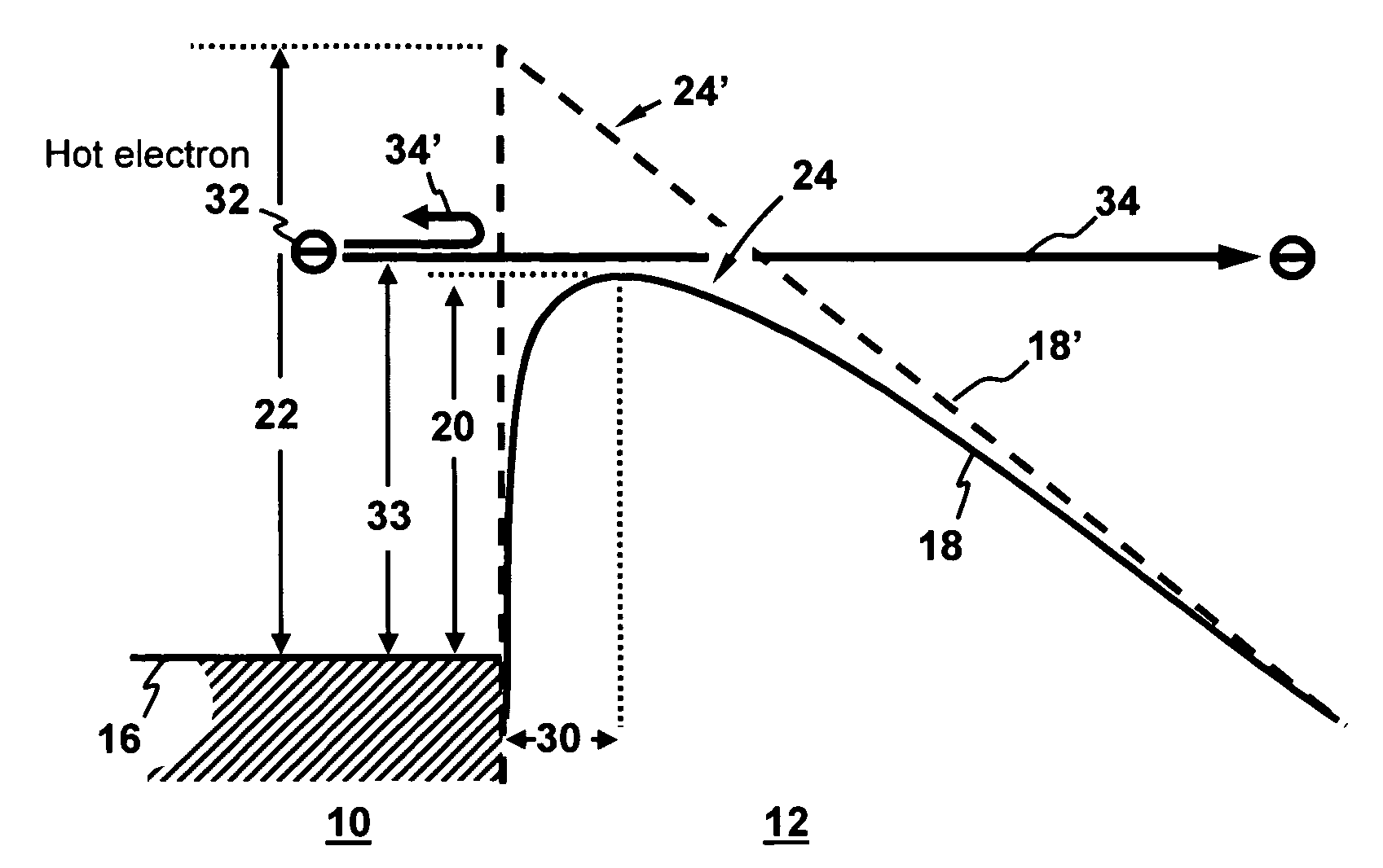
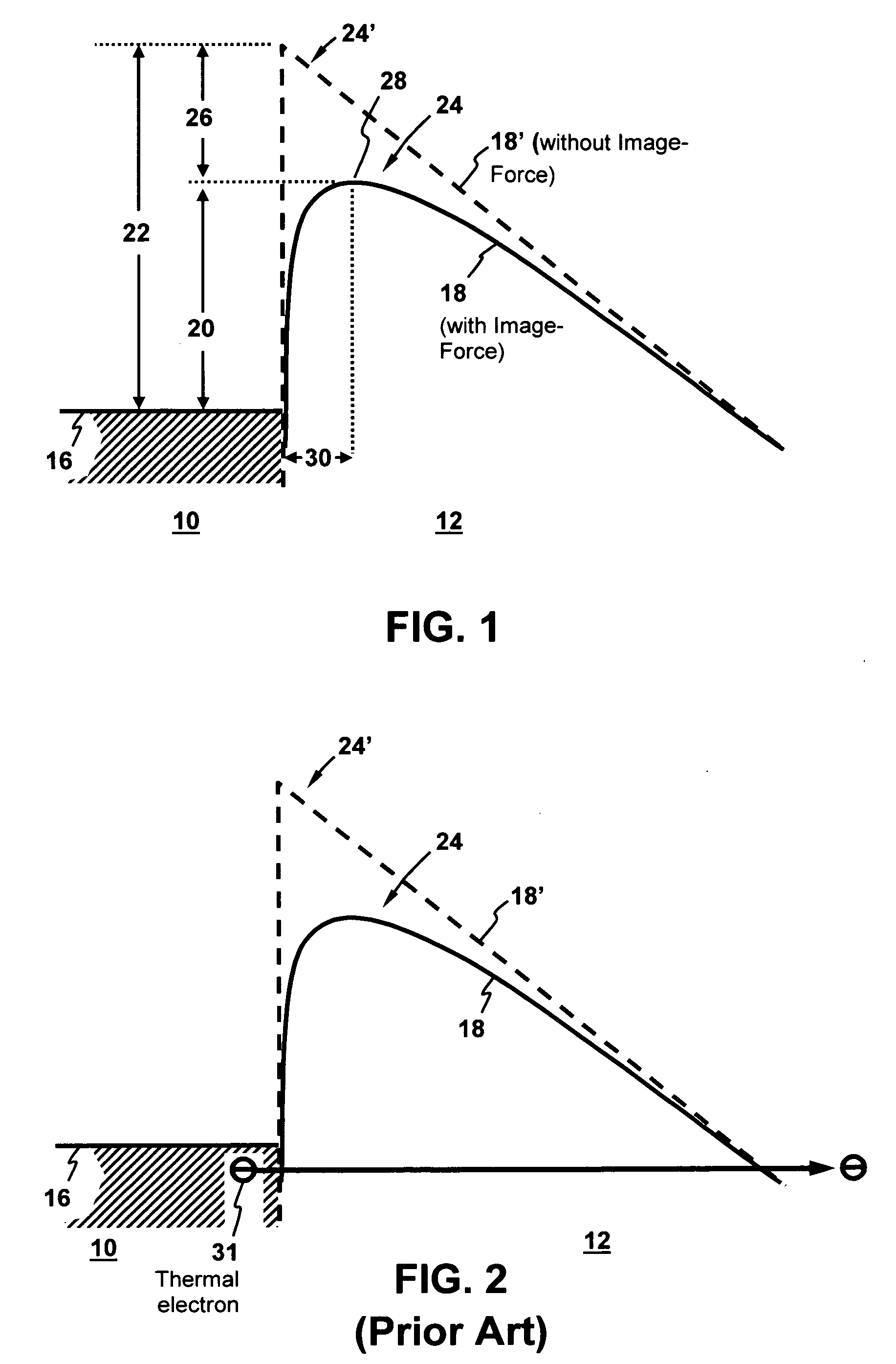
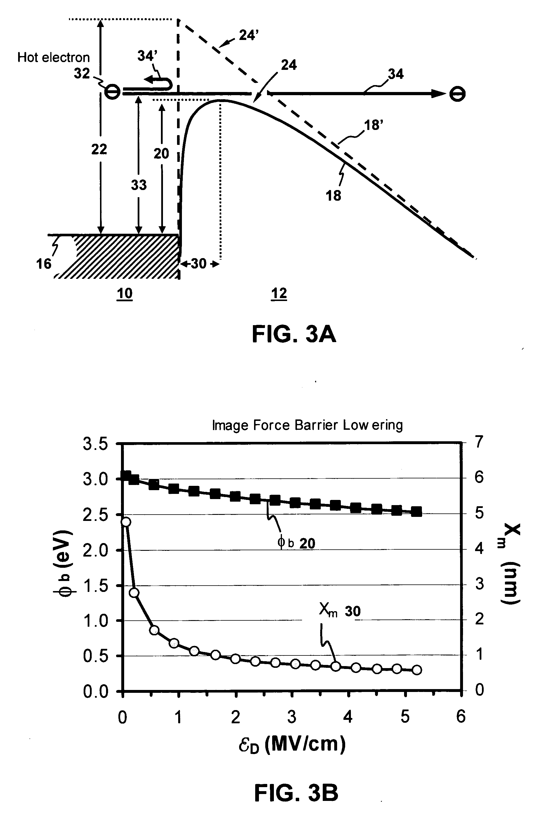
RELATED APPLICATIONS [0001] This application claims the benefit of U.S. Provisional Patent Application Ser. No. 60 / 585,238 filed Jul. 1, 2004 (Attorney Docket No. 2004-2) and U.S. Provisional Patent Application Ser. No. 60 / 626,326 filed Nov. 8, 2004 (Attorney Docket No. 2004-5). This application is a Continuation-In-Part of U.S. patent application Ser. No. 11 / 007,907 filed on Dec. 8, 2004, entitled “METHOD AND APPARATUS FOR NONVOLATILE MEMORY”. This application is also a Continuation-In-Part of U.S. patent application Ser. No. 11 / 120,691 filed on May 2, 2005, entitled “ELECTRICALLY ALTERABLE MEMORY CELL”.TECHNICAL FIELD [0002] The present invention relates to semiconductor device and semiconductor memory device. More particularly, the present invention relates to methods and apparatus on transporting charges in these devices. BACKGROUND OF THE INVENTION [0003] Image-Force is a well-known subject such as described in a publication by Sze, entitled “Physics of Semiconductor Devices,” ...

Claims


Application Information

Patent Timeline
Patent Type & Authority Applications(United States)
IPC IPC(8): H01L29/745
CPCG11C16/0416H01L21/28273H01L27/115H01L27/11521H01L27/11568H01L29/792H01L29/513H01L29/7881H01L29/7883H01L29/7885H01L29/42324H01L29/40114H10B69/00H10B41/30H10B43/30
Inventor WANG, CHIH-HSIN
Owner MARVELL ASIA PTE LTD
Why Eureka
Try Eureka