Supercharge Your Innovation With Domain-Expert AI Agents!

Taped lead frames and methods of making and using the same in semiconductor packaging

a lead frame and semiconductor technology, applied in the field of lead frame, can solve the problems of handling flaws, damage and distortion, flimsy finger-like portions of lead frame, lack of structural rigidity of conventional lead frame, etc., and achieve the effect of enhancing rigidity and supporting

Inactive Publication Date: 2006-01-05
UNISEM M BERHAD
View PDF50 Cites 50 Cited by
  • Summary
  • Abstract
  • Description
  • Claims
  • Application Information

AI Technical Summary

Benefits of technology

[0008] A plurality of electronic packages may be formed using the array of taped lead frames. In this method, a plurality of integrated circuit chips are attached and electrically connected to each lead frame on the array. Thereafter, an encapsulant is applied over the lead frames and the street regions on the tape. In one embodiment, the encapsulating step includes applying the encapsulant material over the lead frame in a controlled manner to flow around the metal features and up to the tape surface without creating any mold flash.
[0011] The metal features may have a thickness of about 1-4 mils or may be less than 1 mil. The tape is made of a disposable and low-cost plastic material, for example, POLYIMIDE, MYLAR, KAPTON, or Fr-4 or alternatively an equivalent carrier that can be removed or disposed like glass-film or shiny plastic film or similar. The tape or alternative carrier may be removed by peeling, dissolving or back patterning. In addition, a stiffener may be incorporated below the lower surface of the tape to provide additional support and rigidity during processing. Where a stiffener is used, it is removed prior to removing the tape during the process.

Problems solved by technology

Conventional lead frames lack structural rigidity.
The finger-like portions of lead frames are quite flimsy and difficult to hold in position during processing.
This leads to handling flaws, damage and distortion during assembly processing.
This can lead to structural defects, such as delamination at the metal-plastic interfaces.

Method used


Image

  • Taped lead frames and methods of making and using the same in semiconductor packaging
  • Taped lead frames and methods of making and using the same in semiconductor packaging
  • Taped lead frames and methods of making and using the same in semiconductor packaging

Examples


Embodiment Construction

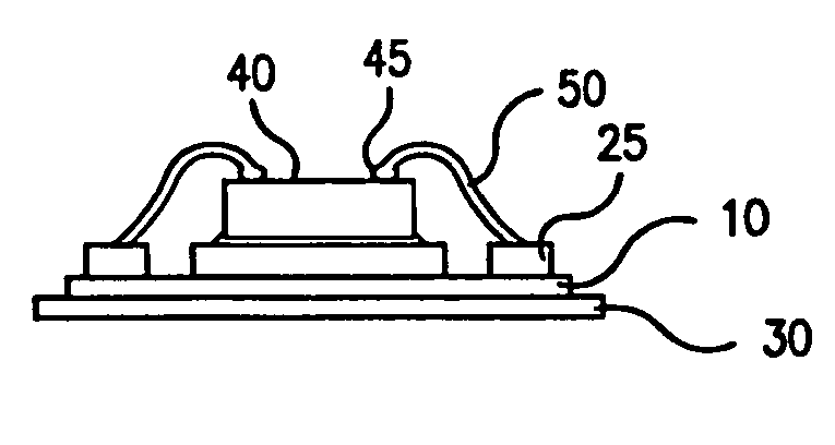
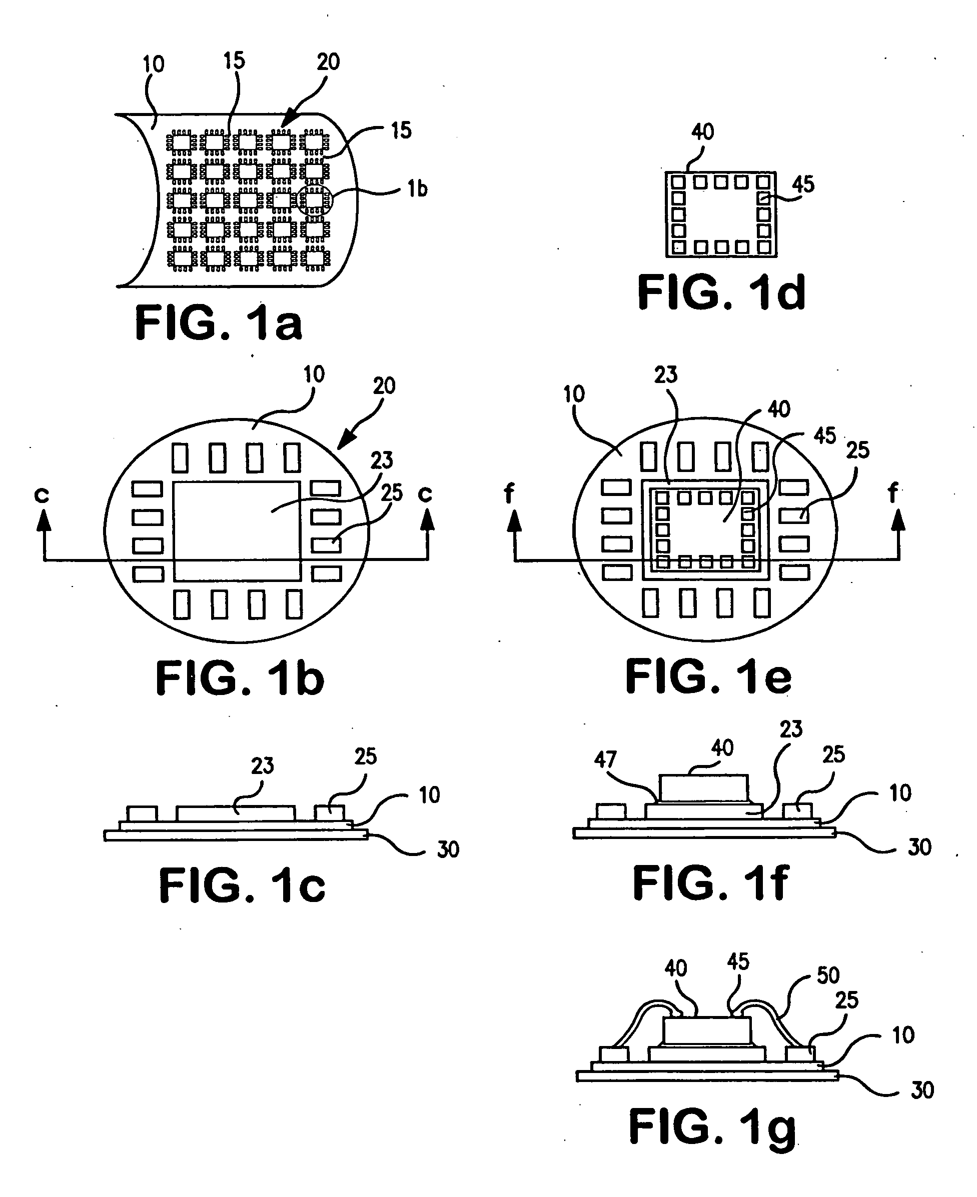
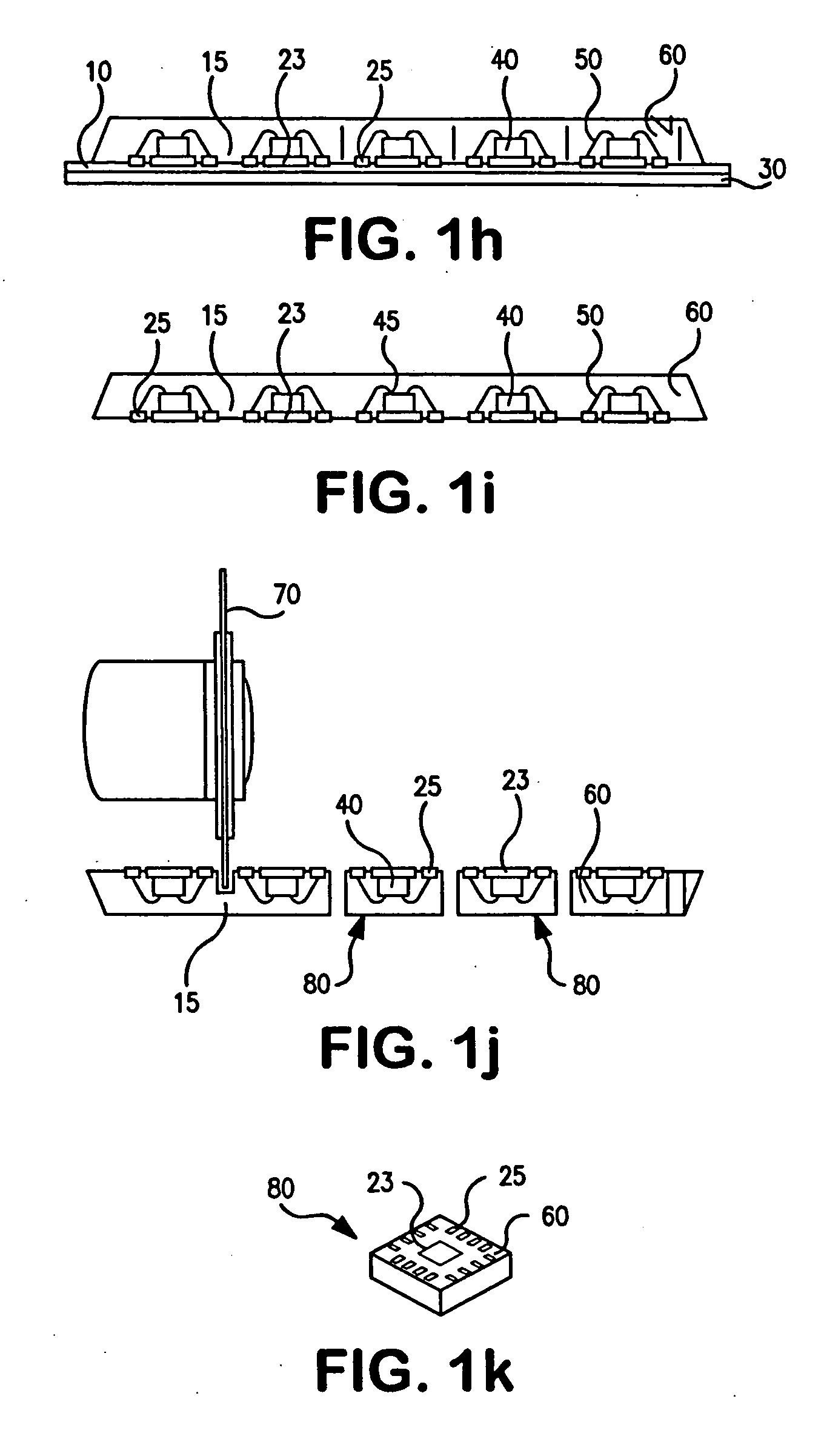
[0063]FIGS. 1a-1o show the forming of an array of taped lead frames for a wire-bonded chip and a method of using the same for forming a taped lead frame package. In a top view shown in FIG. 1a, a strip of metal film is attached to tape (10). The attachment of the tape to the metal film can be accomplished in a number of ways, including conventional lamination techniques, or using an adhesive. Alternatively, a metal film can be screen printed onto a disposable tape or film, including glass film carrier to achieve a thinner package. The metal film is then patterned to form an array of lead frames (20) with each metal feature as shown in FIG. 1a. As shown in FIGS. 1b and 1c, each lead frame comprises a plurality of metal features including chip pad (23) and a set of lead contacts (25) surrounding the chip pad. The areas comprising features of the chip pad (23) and lead contacts (25) is collectively referred to as a chip site. A stiffener (30) optionally may be disposed on the lower sur...


PUM


Abstract

The invention provides a taped lead frame for use in manufacturing electronic packages. The taped lead frame is composed of a tape and a lead frame formed from a plurality of individual metal features attached to the tape and arranged in a footprint pattern. The method of making the invention enables the thickness of conventional frames to shrink significantly to result in thinner packages for improved heat dissipation and shorter geometries for improved electrical performance. A plurality of such lead frames are arranged in an array on a sheet of tape and each lead frame is separated from surrounding lead frames by street regions on the tape such that no metal feature extends into a street region. Integrated circuit chips are attached and electrically connected to the lead frames and an encapsulant is applied, cured and dried over the lead frames and the street regions. Thereafter, the tape is removed and the lead frames are singulated by cutting through the encapsulant in the street regions to form individual packages. Singulation occurs in the street regions and does not cut into any metal feature forming the lead frame.

Description

FIELD OF THE INVENTION [0001] The present invention generally concerns lead frames and the use thereof in the manufacture of packages containing electronic components. In particular, the invention concerns a taped lead frame and a method for making and using the same in creating semiconductor electronic packages. BACKGROUND OF THE INVENTION [0002] Lead frames are typically made by etching or stamping a metal film to specific shapes and dimensions. Finely configured lead frames often resemble very delicate embroidery, or stencil-like metal structures. Such conventional lead frames are used in the industry to create a variety of chip packages, including wire bonded and flip-chip packages. [0003] Conventional lead frames lack structural rigidity. The finger-like portions of lead frames are quite flimsy and difficult to hold in position during processing. This leads to handling flaws, damage and distortion during assembly processing. [0004] In automated processes for making chip size pa...

Claims


Application Information

Patent Timeline
Patent Type & Authority Applications(United States)
IPC IPC(8): H01L23/495H01L21/44H01L21/56H01L21/68H01L23/31H01L23/498
CPCH01L21/561H01L2924/01023H01L23/3107H01L23/4985H01L24/97H01L2224/48091H01L2224/48247H01L2224/48465H01L2224/73265H01L2224/81001H01L2224/83001H01L2224/85001H01L2224/92247H01L2224/97H01L2924/01029H01L2924/01033H01L2924/01046H01L2924/01078H01L2924/01079H01L2924/01082H01L2924/01322H01L2924/14H01L21/568H01L2924/01019H01L2924/01006H01L2924/01005H01L2224/32245H01L2224/16245H01L24/48H01L2924/01087H01L24/17H01L2224/85H01L2924/00014H01L2224/83H01L2224/81H01L2924/00012H01L2924/00H01L2924/12042H01L24/73H01L2224/05599H01L2224/45099H01L2224/85399H01L2924/181H01L2224/45015H01L2924/207H01L23/495
Inventor ISLAM, SHAFIDULSAN ANTONIO, ROMARICO SANTOSGULTOM, LENNY CHRISTINA
Owner UNISEM M BERHAD
Features
  • R&D
  • Intellectual Property
  • Life Sciences
  • Materials
  • Tech Scout
  • Unparalleled Data Quality
  • Higher Quality Content
  • 60% Fewer Hallucinations
Learn More