Method of and apparatus for manufacturing semiconductor device

a semiconductor device and manufacturing method technology, applied in the direction of semiconductor/solid-state device manufacturing, electric devices, basic electric elements, etc., can solve the problems of not being able to avoid the damaged layers that remain, affecting the reliability of semiconductor devices that are produced, and remaining damaged layers that have been chemically damaged

Inactive Publication Date: 2006-01-05
FUKUNAGA AKIRA +1
View PDF26 Cites 2 Cited by
  • Summary
  • Abstract
  • Description
  • Claims
  • Application Information

AI Technical Summary

Benefits of technology

[0029] The chemical liquid may be supplied to the surface of the substrate as by dipping the substrate in the chemical liquid, supplying the chemical liquid to the surface (upper surface) of the substrate while the substrate is being held with its surface facing upwardly, or spraying the chemical liquid from e.g., a spray to the surface (lower surface) of the substrate while the substrate is being held with its surface facing downwardly with a spray. As described above, portions of the interconnect which are not damaged may possibly be dissolved by the oxygen in the atmosphere, depending on the chemical liquid used to dissolve the damaged layer. In this case, the chemical liquid needs to be removed from the surface of the substrate immediately after the damage restoring process. The substrate can be rinsed more easily and the applied chemical liquid can be removed with greater ease in the process of spraying the chemical liquid from e.g., a spray to the surface (lower surface) of the substrate while the substrate is being held with its surface facing downwardly, than the process of dipping the substrate in the chemical liquid or the process of supplying the chemical liquid to the surface (upper surface) of the substrate while the substrate is being held with its surface facing upwardly. Alternatively, the environment in which the spray is applied to the substrate and / or the environment in which the substrate is rinsed may be filled with an inactive gas to eliminate the effect of the oxygen in the atmosphere during the damage restoring process.
[0030] If a process subsequent to the restoration of the damaged layer is an electroless plating process for forming a protective film while the substrate is being held with its surface facing downwardly, then the damaged layer is restored while the substrate is being held with its surface facing downwardly. In this manner, the protective layer can subsequently be formed on the substrate by electroless plating without changing the orientation of the substrate.

Problems solved by technology

On the exposed surfaces of the flattened copper interconnects, there remain damaged layers which have been chemically damaged by the oxidizing agent or the like or physically damaged by the polishing agent or the like.
Though some attempts are made to minimize such damage in the flattening process, it is not possible to avoid the damaged layers that remain left on the surfaces of interconnects either chemically or physically because the oxide layer is formed and the surface is flattened by physically removing the oxide layer.
As finer interconnects are formed, the damaged layers that remain on the surfaces of exposed interconnects tends to adversely affect the reliability of semiconductor devices that are produced.
Such corrosion wastage is responsible for a reduction in the reliability of the semiconductor device due to an increase in the interconnect resistance, poor adhesion between the interconnect material and a film formed thereon, etc.
However, as the polishing process has been improved to reduce excessive polishing in view of finer design rules, e.g., interconnect sizes of less than 0.1 μm, the corrosion wastage that has been concealed has begun to surface, tending to affect the reliability of semiconductor devices.

Method used


Image

  • Method of and apparatus for manufacturing semiconductor device
  • Method of and apparatus for manufacturing semiconductor device
  • Method of and apparatus for manufacturing semiconductor device

Examples


Embodiment Construction

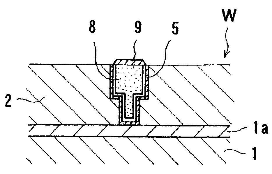
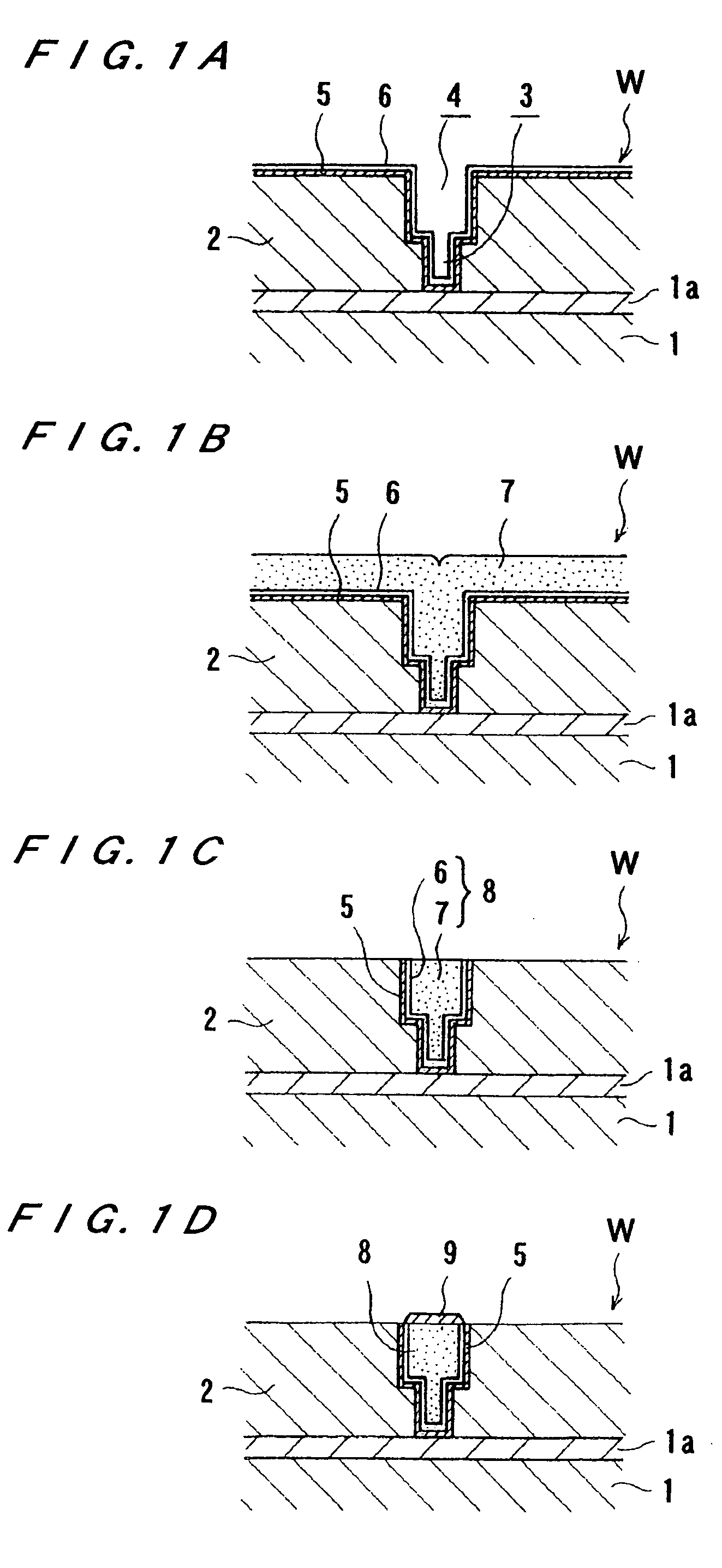
[0104] Preferred embodiments of the present invention will be described in detail below. In the embodiments described below, the present invention is applied to a semiconductor device manufacturing apparatus which embeds copper as an interconnect material in fine interconnect recesses defined in a surface of a substrate, such as a semiconductor wafer or the like, to form interconnects composed of a copper film. However, the present invention is also applicable to semiconductor device manufacturing apparatus which employs interconnect materials other than copper.

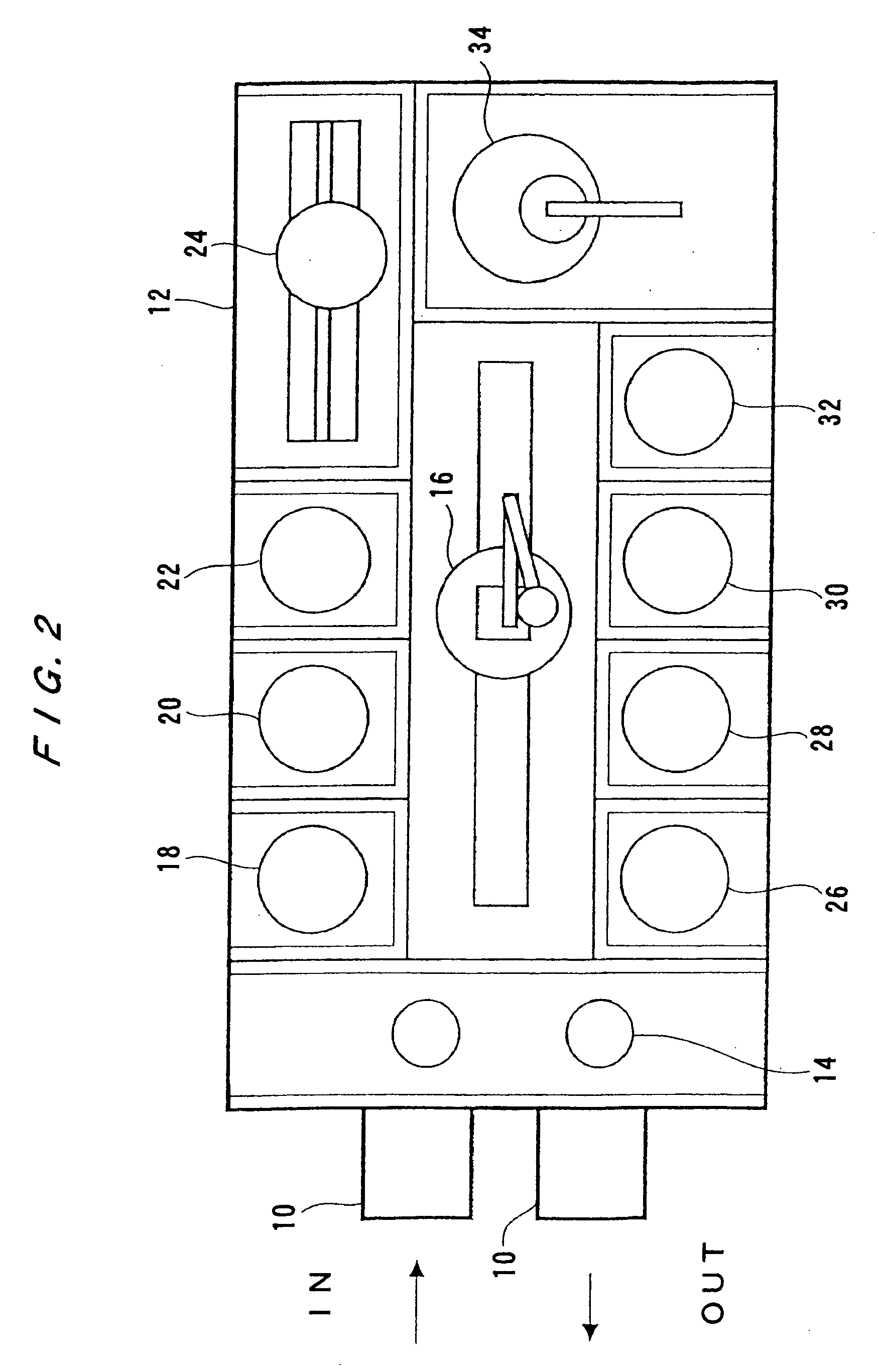
[0105]FIG. 2 shows in plan a semiconductor device manufacturing apparatus according to an embodiment of the present invention. As shown in FIG. 2, the semiconductor device manufacturing apparatus has a rectangular housing 12 to which transport boxes 10 such as a SMIF box for housing a number of substrates such as semiconductor wafers therein are detachably mounted. The housing 12 houses therein a loading / unloading station 14...


PUM


Abstract

A damaged layer which is necessarily produced on the exposed surface of an interconnect by flattening of a surface of a substrate for forming interconnect according to a damascene process is restored, making it possible to manufacture semiconductor devices with a high yield. A semiconductor device is manufactured by preparing a substrate having an interconnect recess formed in ah interlevel dielectric, depositing an interconnect material on the surface of the substrate to embed the interconnect material in the interconnect recess, removing the interconnect material excessively formed on the surface of the substrate to flatten the surface of the substrate, thereby forming an interconnect of the interconnect material, and restoring a damaged layer formed on the exposed surface of the interconnect.

Description

BACKGROUND OF THE INVENTION [0001] 1. Field of the Invention [0002] The present invention relates to a method of and an apparatus for manufacturing a semiconductor device, and more particularly to a method of and an apparatus for manufacturing a semiconductor device by filling fine interconnect recesses such as interconnect trenches, contact holes, etc. previously formed in an interlevel dielectric deposited on a surface of a substrate, such as a semiconductor wafer or the like, with an interconnect material (conductive metal) such as aluminum, copper, silver, or their alloy, and thereafter removing an extra metal to flatten the surface of the substrate, thereby forming embedded interconnects on the surface of the substrate. [0003] 2. Description of the Related Art [0004] There has been employed a damascene process for embedding an interconnect material (conductive metal) into interconnect trenches, contact holes, etc. as an interconnect forming process for manufacturing semiconduct...

Claims


Application Information

Patent Timeline
Patent Type & Authority Applications(United States)
IPC IPC(8): H01L21/8238H01L21/02H01L21/288H01L21/306H01L21/321H01L21/3213H01L21/44H01L21/4763H01L21/768
CPCH01L21/02074H01L21/02087H01L21/0209H01L21/288H01L21/76879H01L21/76843H01L21/76849H01L21/76877H01L21/7684
Inventor FUKUNAGA, AKIRATSUJIMURA, MANABU
Owner FUKUNAGA AKIRA
Why Eureka
Try Eureka