

Expanding method and expanding device
a technology of expanding device and adhesive sheet, which is applied in the direction of mechanical vibration separation, electric/magnetic/electromagnetic heating, manufacturing tools, etc., can solve the problems of reducing degrading the good chips t or compromising the reliability of finished products, so as to reduce the operating rate of the dicing device. , the spacing between the individual
- Summary
- Abstract
- Description
- Claims
- Application Information
AI Technical Summary
Benefits of technology
Problems solved by technology
Method used
Image

Examples
first embodiment
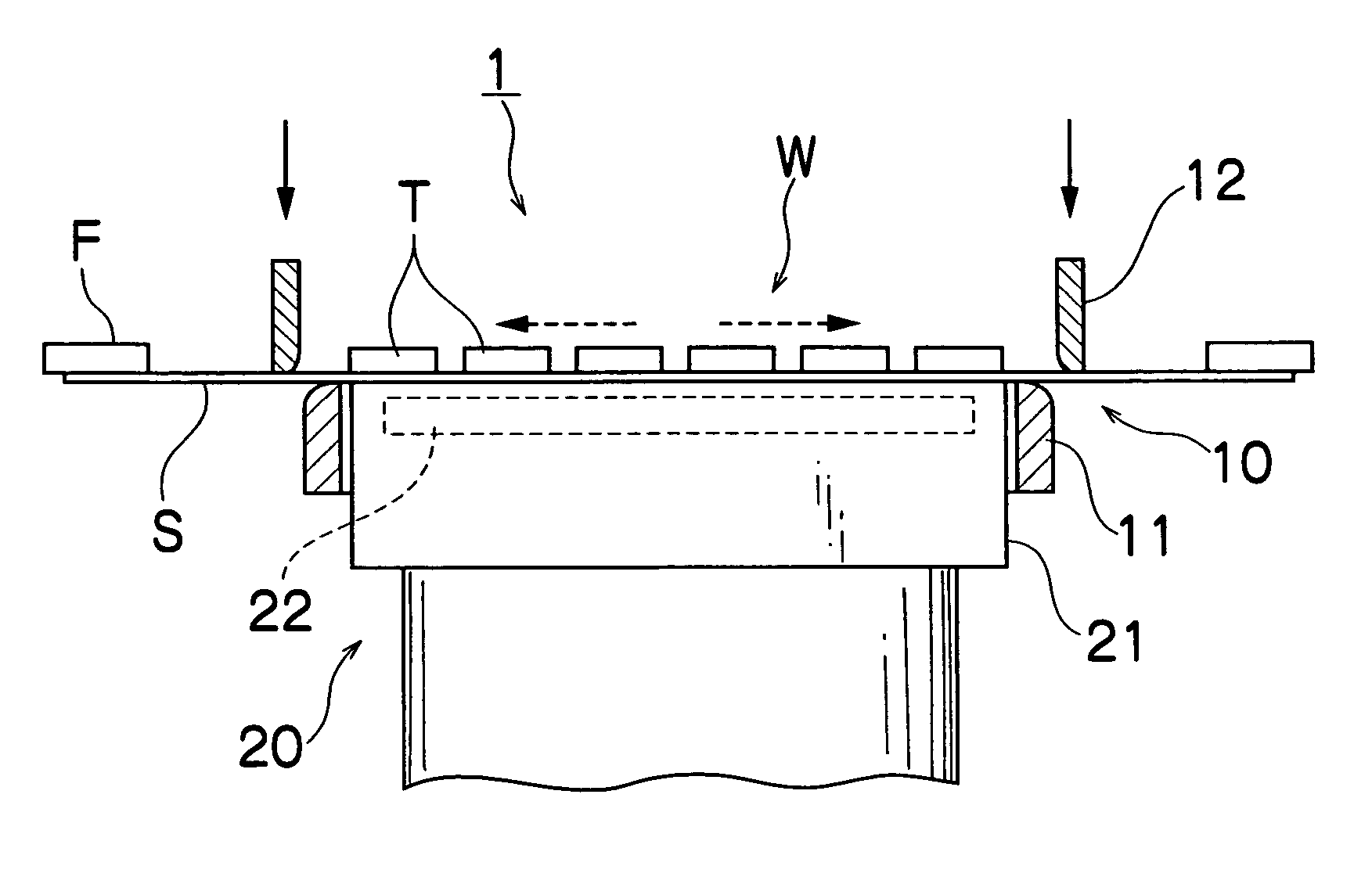
[0087]FIG. 1 shows an expanding device according to the invention. The expanding device 1 includes expanding means 20 constituted by a heating stage 21, and expansion maintaining means 10 constituted by an inner ring 11 and an outer ring 12.
[0088] A heater 22 is incorporated in the heating stage 21 near an upper surface thereof and set so as to heat the upper surface of the heating stage 21 to a predetermined temperature. The inner ring 11 is detachably placed on an outer periphery of the heating stage 21. An inner diameter of the outer ring 12 is sized to be firmly fitted over an outer periphery of the inner ring 11 intercalated an adhesive sheet S. The outer ring 12 is vertically moved by unshown drive means.
[0089] Next, as a first embodiment of an expanding method according to the invention, operations of the expanding device 1 thus configured will be described. A wafer W is cut into individual chips T, T, . . . by dicing and then placed on the heating stage 21. When the wafer W...
second embodiment
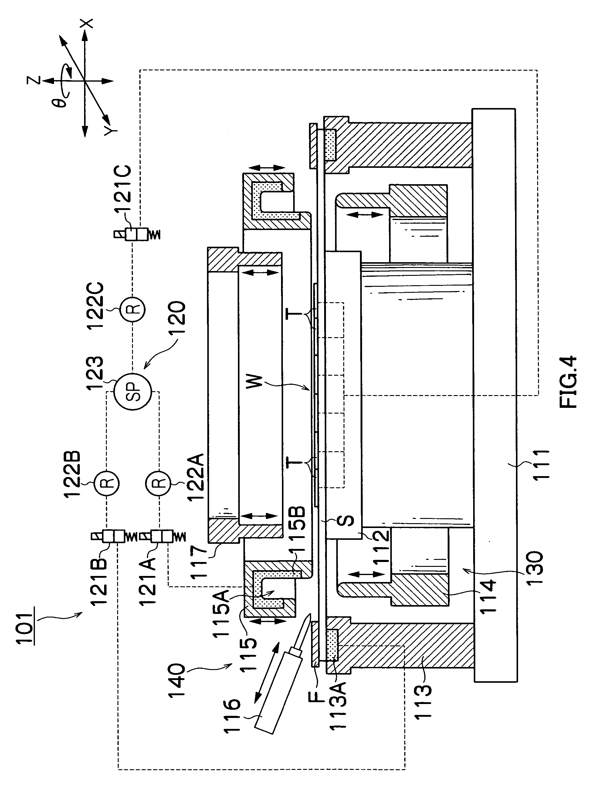
[0092]FIG. 4 shows an expanding device according to the invention. The expanding device 101 includes an XY θ table 111, a chuck stage 112, a frame chuck 113, a pressure member 114, a housing 115, an ultrasonic welding tool 116 as a welding tool, and a pressing ring 117, or the like, expanding means 130 includes the frame chuck 113, the housing 115, and the pressure member 114, or the like, and expansion maintaining means 140 includes the housing 115, the pressing ring 117, and the ultrasonic welding tool 116, or the like.
[0093] The XY θ table 111 is moved in XY directions in FIG. 4 and rotated through 0 by an unshown drive device. The chuck stage 112 and the frame chuck 113 are mounted to the XY θ table 111. A porous member 113A is embedded in an upper surface of the frame chuck 113, and connected to a pressure reducing pump 123 that constitutes pressure reducing means 120 through a solenoid valve 121B and a regulator 122B so as to suck a frame F.
[0094] An unshown porous member is ...
third embodiment
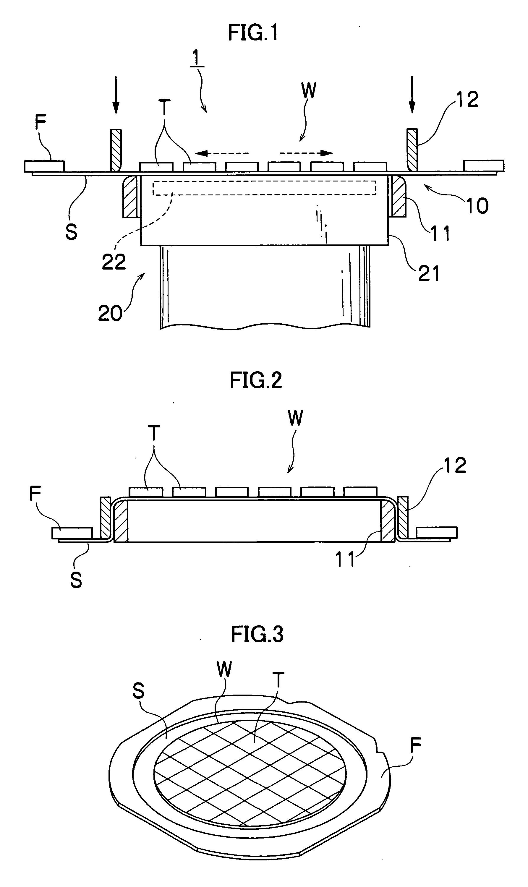
[0113]FIG. 8 illustrates an expanding device according to the invention, and is a front view of part of the expanding device and a state where a conveying device including expanding means is positioned in a dicing area of a dicing device. FIG. 9 is a plan view thereof.
[0114] As shown in FIGS. 8 and 9, an expanding device 201 includes conveying means 230, expanding means 233 mounted to the conveying means 230, sheet clamping means 234, and sheet loose part securing means 201A that is expansion maintaining means provided in a below described welding area (a different area), or the like.
[0115] The conveying means 230 conveys a wafer W that is a plate-like article mounted to a frame through an adhesive sheet S together with a chuck stage 206 of the dicing device from the dicing area to the welding area (the different area), and includes a rotation arm 231 that is rotated around a shaft 231B and vertically moved by unshown drive means, two support beams 231A and 231A, and four forks 232...
PUM
| Property | Measurement | Unit |
|---|---|---|
| thickness | aaaaa | aaaaa |
| thickness | aaaaa | aaaaa |
| thickness | aaaaa | aaaaa |
Abstract
Description
Claims
Application Information