

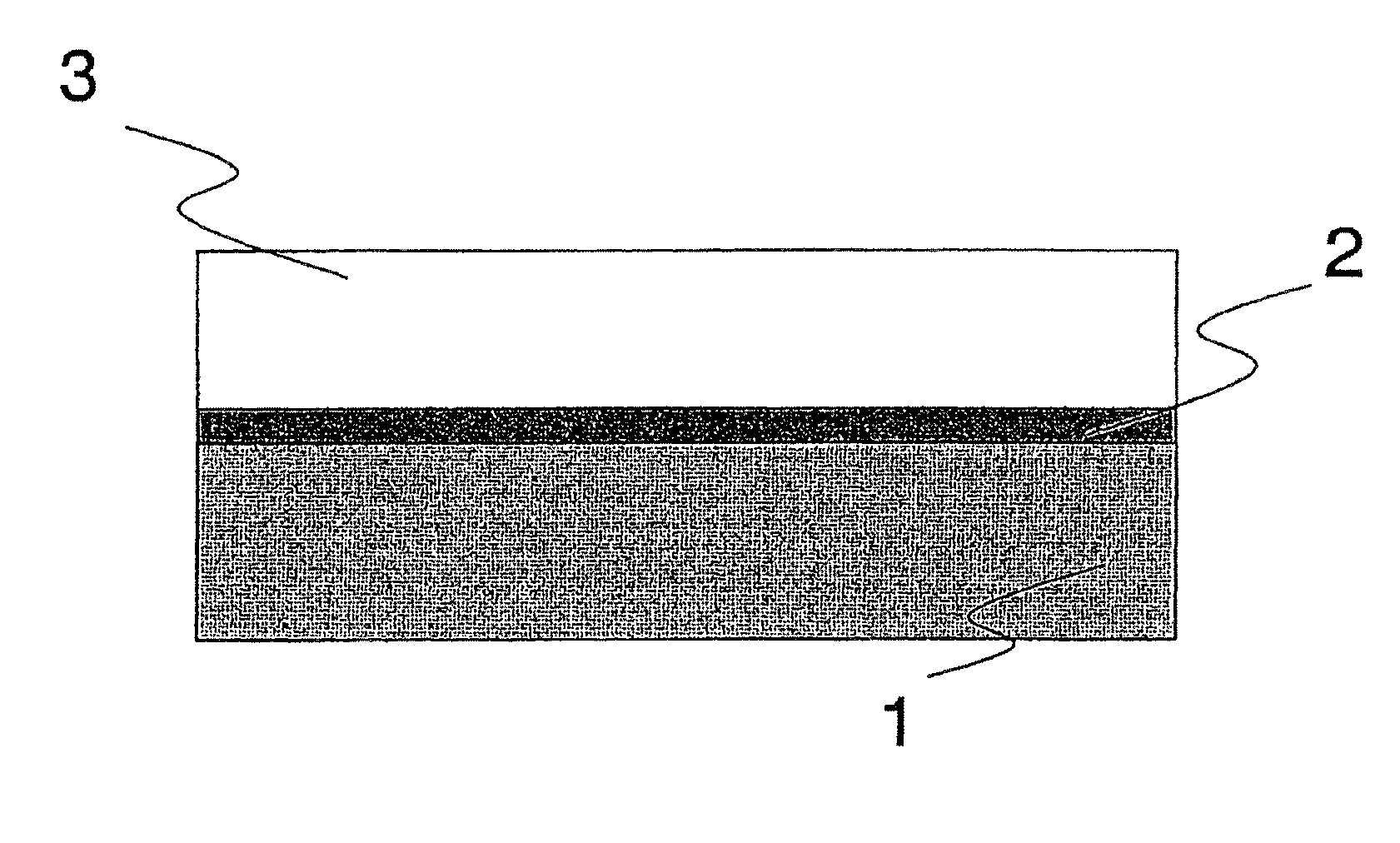
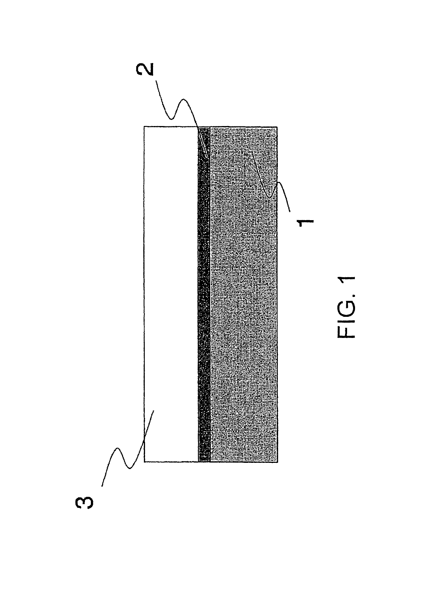
Protective film structure of metal member, metal component employing protective film structure, and equipment for producing semiconductor or flat-plate display employing protective film structure
a protective film and metal member technology, applied in the direction of instruments, superimposed coating processes, natural mineral layered products, etc., can solve the problems of increasing the number of apparatuses and increasing the investment amount, and it is difficult to realize small-scale production lines. , to achieve the effect of reducing the contamination of the substrate, preventing surface corrosion, and excellent corrosion resistan
- Summary
- Abstract
- Description
- Claims
- Application Information
AI Technical Summary
Benefits of technology
Problems solved by technology
Method used
Image

Examples
examples
[0045]Examples of this invention will be described hereinbelow. Naturally, this invention is not limited to the following examples.
[0046]The analysis conditions in the following examples and comparative examples are as follows:
(Analysis Condition 1) Scanning Electron Microscope (hereinafter abbreviated as “SEM Analysis”)
Apparatus: JE6700 produced by JEOL
(Analysis Condition 2) Fourier Transform Infrared Spectroscopic Analysis (hereinafter abbreviated as “FT-IR Analysis”)
Apparatus: Digilab Japan
(Analysis Condition 3) Atmospheric Pressure Ionization Mass Spectrometry (hereinafter abbreviated as “APIMS Analysis”)
Apparatus: UG-302P produced by Renesas Eastern Japan
[0047]In this example, use was made of a JIS A5052 material as aluminum, special grade reagents produced by Wako Pure Chemical Industries, Ltd. as tartaric acid and ethylene glycol, and an EL-grade chemical produced by Mitsubishi Chemical Corporation as aqueous ammonia.
[0048]Anodic oxidation was performed using a source meter (...
PUM
| Property | Measurement | Unit |
|---|---|---|
| pH | aaaaa | aaaaa |
| pH | aaaaa | aaaaa |
| thickness | aaaaa | aaaaa |
Abstract
Description
Claims
Application Information