Substrate supporting structure for semiconductor processing, and plasma processing device
a supporting structure and semiconductor technology, applied in the direction of chucks, manufacturing tools, mechanical equipment, etc., can solve the problems of increasing the footprint of the semiconductor processing device, reducing the productivity of the semiconductor device, and incurred substantial cost increases, so as to reduce the cost
- Summary
- Abstract
- Description
- Claims
- Application Information
AI Technical Summary
Benefits of technology
Problems solved by technology
Method used
Image
Examples
first embodiment
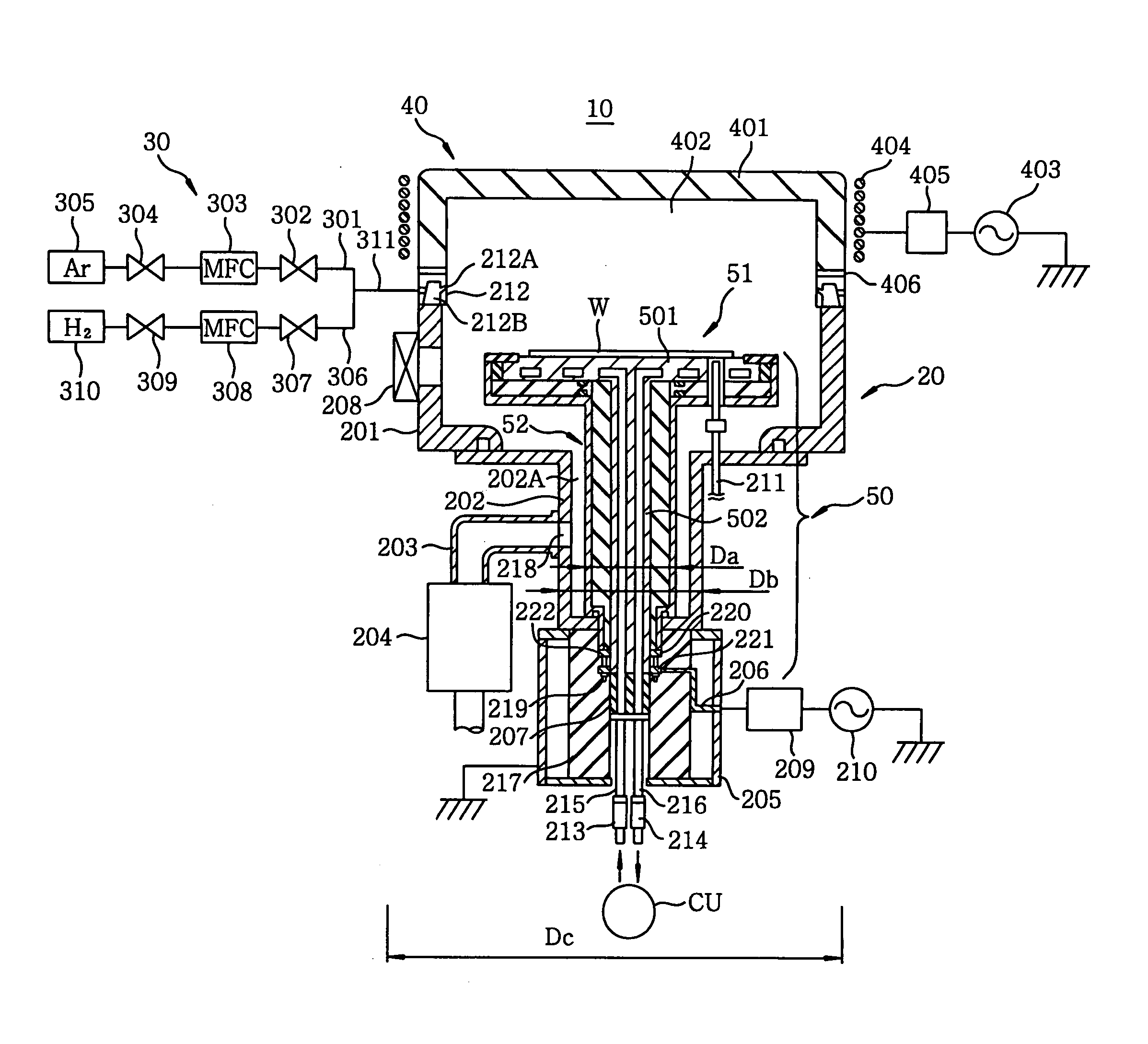
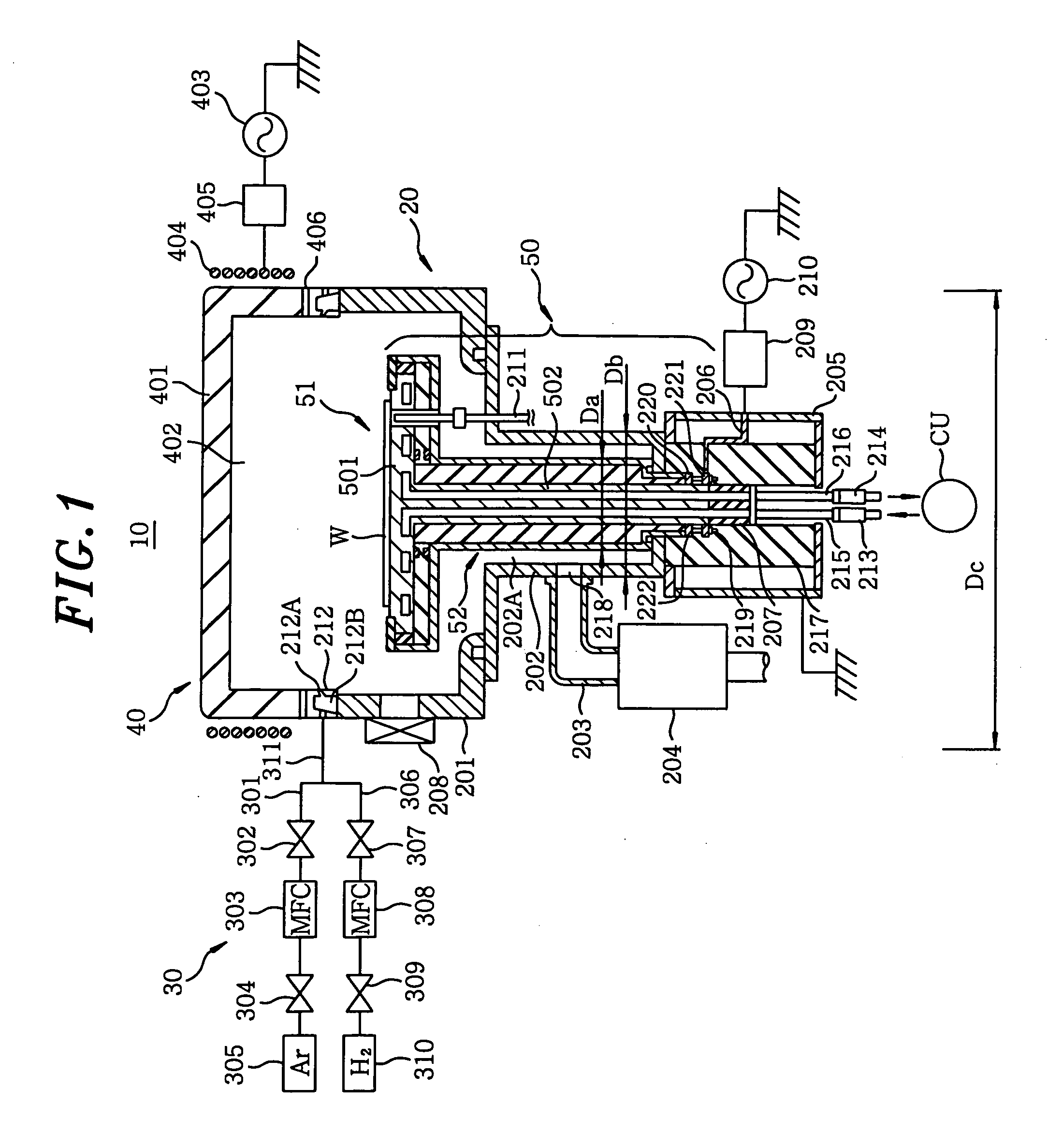
[0026]FIG. 1 is a configuration view showing a plasma processing device including a substrate supporting structure for semiconductor processing in accordance with a first embodiment of the present invention. A plasma processing device 10 is configured to perform a sputter etching or a reactive etching on a silicon oxide film, a metal oxide film or the like, which is formed on a semiconductor wafer as a substrate to be processed.
[0027] As shown in FIG. 1, the plasma processing device 10 includes a processing chamber 20 for receiving thereinto a substrate W to be processed. To the processing chamber 20, a gas supply unit 30 for supplying a processing gas thereinto is coupled. An excitation mechanism 40 for converting the processing gas into a plasma is disposed at an outer upper side of the processing chamber 20. A mounting table 51 of a substrate supporting structure 50 for supporting the substrate W to be processed is disposed at an inner lower side of the processing chamber 20.
[0...
second embodiment
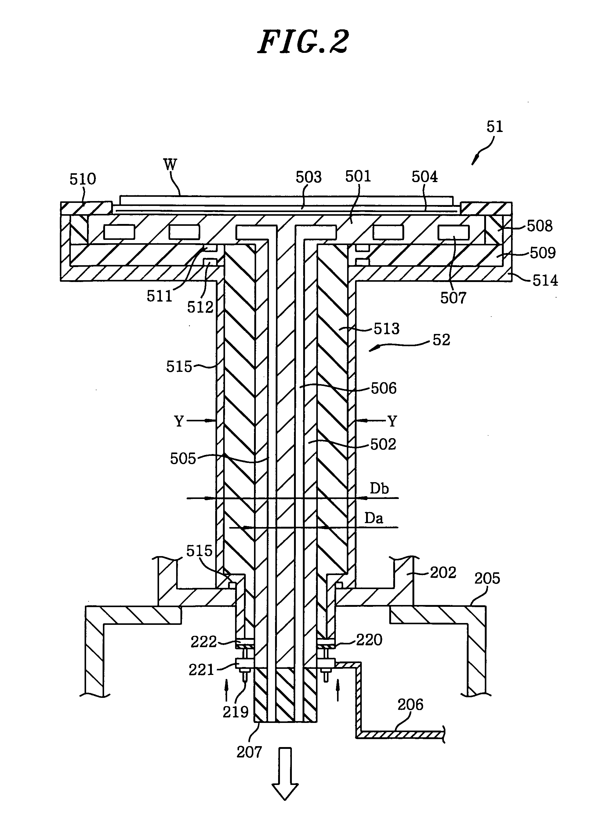
[0085] In the aforementioned plasma processing device 10, if the metal oxide formed on the surface of metal, e.g., copper, aluminum or the like, is etched, metal removed from the substrate W to be processed is scattered. Scattered metal is deposited onto the top surface of the insulating focus ring 510 around the substrate W to be processed, and thus, forming a metal film. If the metal film is grown, a discharge path may be formed between the substrate to be processed (semiconductor wafer) W and the conductive cover (pedestal conduction layer) 514, which is grounded, through the metal film. In this case, since charged particles on the metal film flow on the cover 514 as a current, there may be incurred a loss of the RF power supplied to the electrode part 501. For the same reason, the processing efficiency is lowered and the processing uniformity is deteriorated due to a decrease in the self-bias or abnormal discharge in the discharge path.
[0086] Further, an electromagnetic configu...
PUM
| Property | Measurement | Unit |
|---|---|---|
| Power | aaaaa | aaaaa |
| Power | aaaaa | aaaaa |
| Frequency | aaaaa | aaaaa |
Abstract
Description
Claims
Application Information


