
Substrate having built-in semiconductor apparatus and manufacturing method thereof

a technology of semiconductor apparatus and built-in substrate, which is applied in the direction of electrical apparatus, semiconductor device details, semiconductor/solid-state device devices, etc., can solve the problems of many build-up layers, high initial percent of defective integrated substrate, and difficult to guarantee kgd, etc., and achieve the effect of reducing the production cost per integrated substrate uni

Inactive Publication Date: 2006-01-12
LAPIS SEMICON CO LTD
View PDF1 Cites 38 Cited by
  • Summary
  • Abstract
  • Description
  • Claims
  • Application Information

AI Technical Summary

Benefits of technology

This design ensures higher yield ratios and reduced production costs by guaranteeing non-defective units and improving the flexibility of wiring connections, while maintaining high-density packaging.

Problems solved by technology

However, a substrate having, e.g., a built-in semiconductor chip has the following problems.
First, in a bare chip state, it is hard to guarantee KGD (Known Good Die: quality assurance chip), i.e., a perfect non-defective unit.
Furthermore, since burn-in, i.e., a pre-use operation in order to find a defect cannot be carried out before building such chips in the substrate, there is known that an initial percent defective of the integrated substrate is high.
Second, when a pitch (or an interval) between pads provided to a semiconductor chip is narrow, many build-up layers are required when building such a chip in a substrate.
Therefore, a product cost per integrated substrate is high, and pulling wirings from pads with a narrow pitch interval to an external terminal on the surface of the integrated substrate becomes complicated.
Therefore, there is fear of a reduction in yield ratio.
Therefore, a product cost in an integrated substrate unit is increased, and there is fear of a reduction in yield ratio due to complexity of pulling wirings from pads with a narrow pitch interval to external terminals on the surface of the integrated substrate.

Method used


Image

  • Substrate having built-in semiconductor apparatus and manufacturing method thereof
  • Substrate having built-in semiconductor apparatus and manufacturing method thereof
  • Substrate having built-in semiconductor apparatus and manufacturing method thereof

Examples


first embodiment

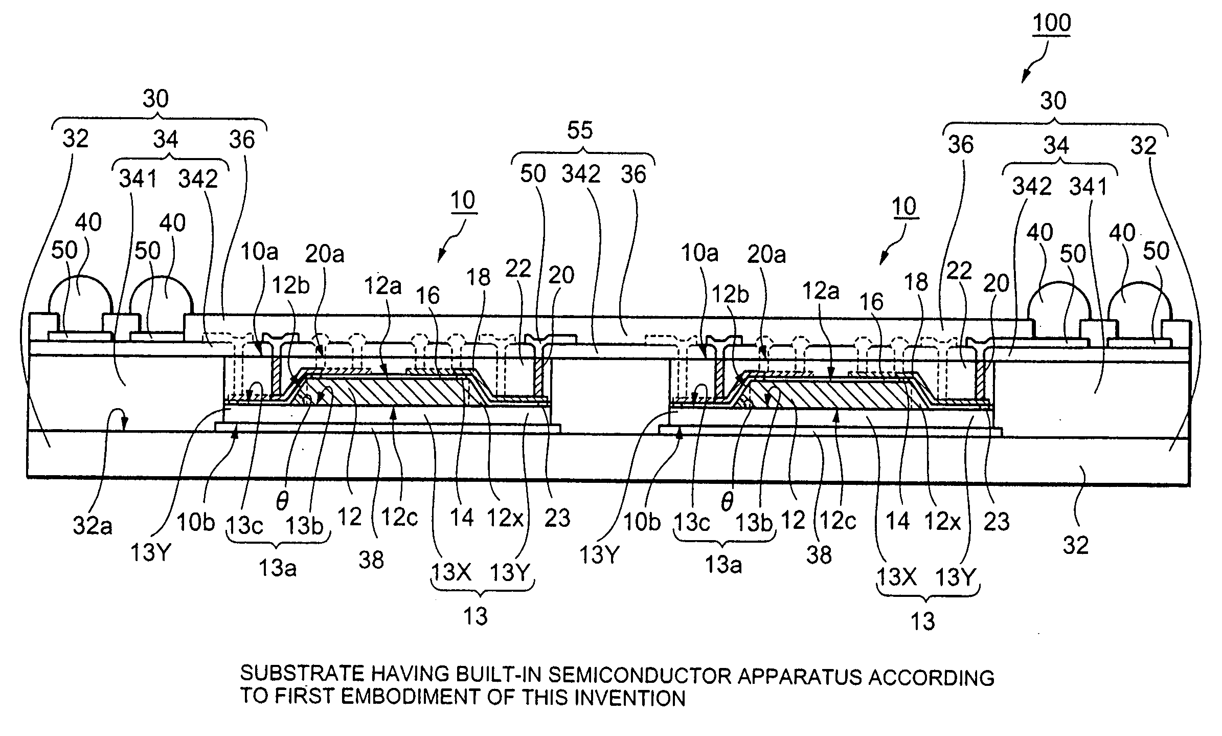
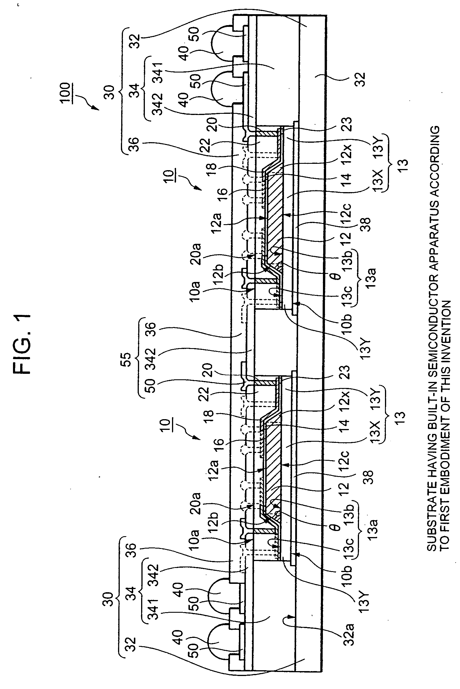
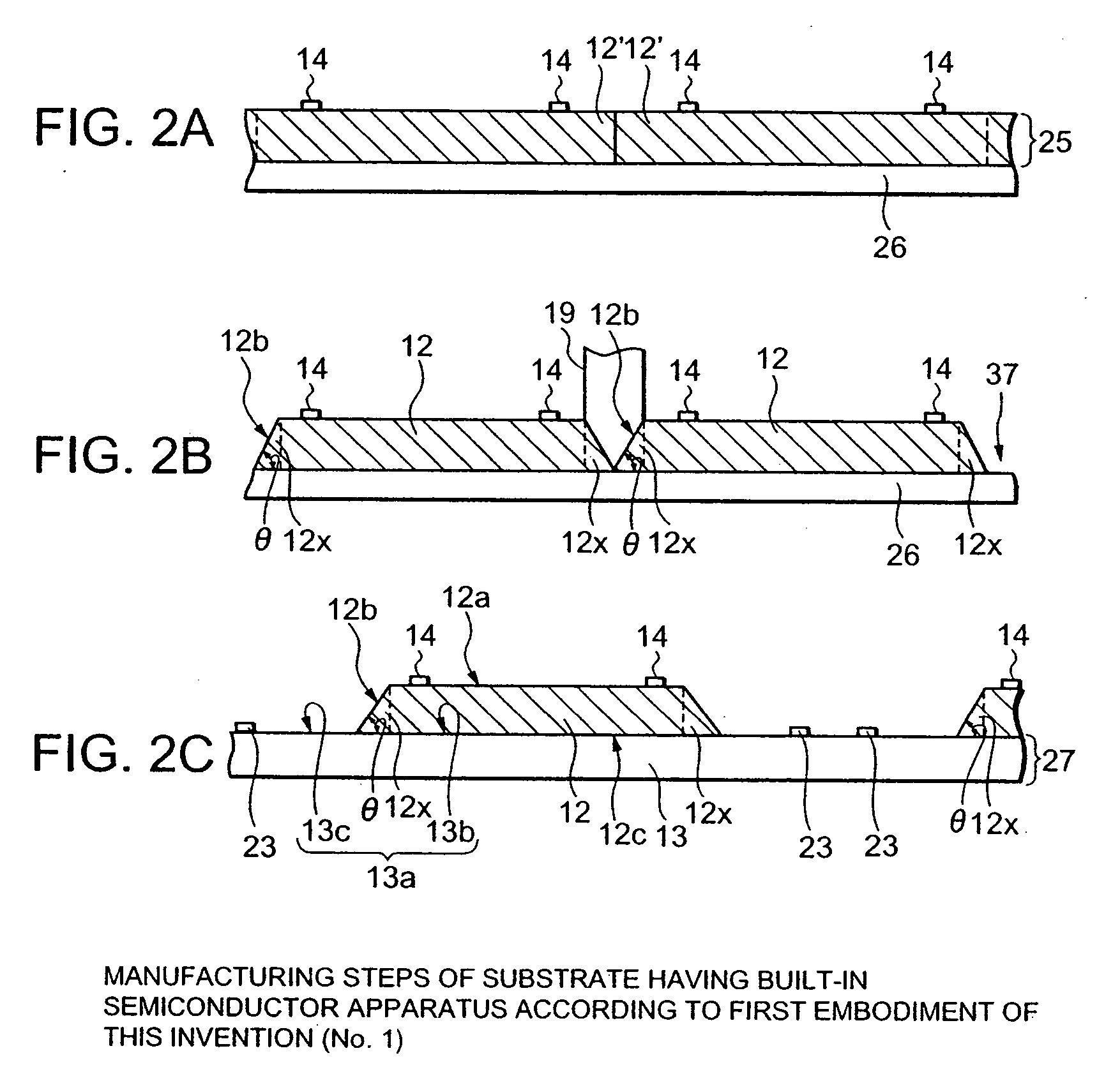
[0049] A substrate having a built-in semiconductor apparatus and a manufacturing method thereof according to the first embodiment will now be described with reference to FIGS. 1 to 5. FIG. 1 is a cross-sectional view schematically illustrating how connections and arrangements of respective constituent elements of a substrate having a built-in semiconductor apparatus 100 are achieved. FIGS. 2 to 5 are process charts illustrating a manufacturing method of the substrate having a built-in semiconductor apparatus 100, and respective drawings of process stages are cross-sectional views schematically showing structures obtained on the process stages.

[0050] As shown in FIG. 1, the substrate having a built-in semiconductor apparatus 100 according to this embodiment comprises a semiconductor apparatus 10, an insulating layer 30 in which the semiconductor apparatus 10 is embedded, an external terminal 40 provided on the insulating layer 30, and an substrate wiring portion 50 which electricall...

second embodiment

[0091] The second embodiment according to the present invention will now be described with reference to FIGS. 6 to 9.

[0092] FIGS. 6 to 9 are schematic cross-sectional views illustrating a substrate having a built-in semiconductor apparatus and a manufacturing method thereof according to this embodiment. It is to be noted that like reference numerals denote the same constituent elements equal to those which have been already described in connection with the first embodiment, thereby eliminating their concrete explanation (this is also the same in each of the following embodiments).

[0093] In this embodiment, a main difference from the first embodiment lies in that a substrate having a built-in semiconductor apparatus 200 is constituted by using a pre-preg hardened layer which includes an electric conductor patterned on a surface thereof and has a pair of hardened pre-pregs in place of the build-up layer.

[0094] As shown in FIG. 6, the substrate having a built-in semiconductor appara...

third embodiment

[0111] The third embodiment according to the present invention will now be described with reference to FIGS. 10 and 11.

[0112] In this embodiment, when manufacturing the substrate having a built-in semiconductor apparatus, a main difference from the second embodiment lies in that a first resin formed plate having holes formed to the pre-preg so as to expose the part of the copper foil opposed to the substrate having built-in semiconductor apparatus is used in the resin formed plate arranging step.

[0113] In the second embodiment, of the surface of the substrate having a built-in semiconductor apparatus 200, it is often the case that the surface on the side where the semiconductor apparatus is embedded in particular is inferior in flatness and may become an irregular surface. That is because the pre-preg at the part corresponding to the semiconductor apparatus is thrusted toward any other area in the thrusting step, but the pre-preg has a lower fluidity since it contains paper or fib...


PUM


Abstract

A substrate having a built-in semiconductor apparatus includes: a semiconductor apparatus which comprises a first semiconductor chip having a first electrode pad formed on a main surface thereof, a protruding portion which is in contact with the first semiconductor chip and protrudes from a side surface of the first semiconductor chip to the outside, an apparatus wiring portion which is provided so as to extend from the first electrode pad onto a surface of the protruding portion, a conductive portion which is in connected with the apparatus wiring portion and provided on the apparatus wiring portion, and a sealing layer which covers the main surface and the surface of the protruding portion so as to expose a top face of the conductive portion; an insulating layer in which the semiconductor apparatus is embedded; an external terminal provided on the insulating layer; and a substrate wiring portion which electrically connects the conductive portion with the external terminal.

Description

[0001] This application is a divisional of U.S. application Ser. No. 10 / 742,940, filed Dec. 23, 2003.BACKGROUND OF THE INVENTION [0002] 1. Field of the Invention [0003] The present invention relates to a substrate having a built-in semiconductor apparatus and a manufacturing method thereof. [0004] This application is counterpart of Japanese patent application, Serial Number 336380 / 2003, filed Sep. 26, 2003, the subject matter of which is incorporated herein by reference. [0005] 2. Description of the Related Art [0006] There has been proposed a substrate having a built-in semiconductor chip to which an active element such as a transistor is formed or a substrate having a built-in passive element such as a capacitor or a resistor with a demand for high-density packaging of an electronic device (see, e.g., patent document 1). [0007] (Patent Document 1) Japanese patent application laid-open No. 2002-170827 [0008] However, a substrate having, e.g., a built-in semiconductor chip has the f...

Claims


Application Information

Patent Timeline
Patent Type & Authority Applications(United States)
IPC IPC(8): H01L21/44H01L21/60H01L23/12H01L23/498H01L23/52H01L23/538H01L25/04H01L25/10H01L25/18
CPCH01L23/49816H01L2224/82007H01L24/24H01L24/82H01L2224/24137H01L2224/24226H01L2224/24998H01L2924/01013H01L2924/01027H01L2924/01029H01L2924/01075H01L2924/01078H01L2924/10157H01L2924/19041H01L2924/19043H01L2924/01005H01L2924/01006H01L2924/01019H01L2924/01023H01L2924/01033H01L2924/01067H01L2924/014H01L24/19H01L23/5389H01L2224/73267H01L2224/04105
Inventor SHIZUNO, YOSHINORI
Owner LAPIS SEMICON CO LTD
Learn More