
Insulation film formation device

a technology of film formation device and film, which is applied in the direction of liquid surface applicators, electrostatic spraying apparatus, coatings, etc., can solve the problems of increasing the footprint of the entire sod system, generating difficulty in the sod system, and poor transfer efficiency of wafers within the sod system. , to achieve the effect of suppressing waste, reducing footprint, and improving substrate transfer efficiency

Inactive Publication Date: 2006-01-19
TOKYO ELECTRON LTD
View PDF12 Cites 18 Cited by
  • Summary
  • Abstract
  • Description
  • Claims
  • Application Information

AI Technical Summary

Benefits of technology

[0018] A first object of the present invention, which has been achieved in view of the situation described above, is to provide an insulating film-forming apparatus, which permits diminishing the footprint and which also permits improving the transfer efficiency of the substrate. Also, a second object of the present invention is to provide an insulating film-forming apparatus that permits suppressing the waste of, for example, a chemical liquid.
[0027] In the insulating film-forming apparatus of the present invention, a plurality of process units required for forming an insulating film are arranged within a single process tower so as to make it possible to decrease the footprint of the insulating film-forming apparatus. Also, the transferring distance of the substrate can be shortened, and the substrate can be transferred efficiently so as to achieve a high through-put. Further, the construction of the process unit arranged within the process tower can be appropriately changed easily in accordance with the object, and the process tower itself can be replaced easily by another process tower in accordance with, for example, the change in the chemical liquid that is used. As a result, the maintenance of the process unit arranged within the process tower and the maintenance of the entire process tower can be performed easily.
[0028] Also, in the insulating film-forming apparatus of the present invention, it is desirable to connect a unit control device included in each of the plural process units arranged within the process tower for controlling the processing of the substrate to a tower control apparatus for controlling a series of processing performed by the plural process units arranged within the process tower. In this case, it is desirable for the tower control apparatus to be constructed to recognize automatically the process unit connected to the tower control apparatus. When the insulating film-forming apparatus is constructed to be capable of automatically detecting the change in the construction of the process unit within the process tower, it is possible to apply the process control to the substrate in the entire insulating film-forming apparatus.
[0029] Further, it is desirable for the insulating film-forming apparatus of the present invention to include at least two substrate process sections that are constructed such that at least one substrate process section is detachable from the other substrate process section. In other words, it is desirable to construct the insulating film-forming apparatus such that an additional substrate process section can be arranged in addition to a single substrate process section that was arranged initially. In this case, it is possible to increase the process capacity of the insulating film-forming apparatus while suppressing the increase in the footprint of the insulating film-forming apparatus as much as possible.
[0030] Further, it is desirable for the coating unit to have a two-stage structure of a coating process section formed in the upper stage and a waste liquid recovery section formed in the lower stage. In this case, it is desirable to arrange in the coating process section a substrate holding mechanism for holding the substrate substantially flat, a chemical liquid supply nozzle for supplying a chemical liquid to the substrate held by the substrate holding mechanism, and a cup surrounding the side surfaces of the substrate held by the substrate holding mechanism and equipped with a chemical liquid discharge port formed in the bottom. It is also desirable to arrange in the waste liquid recovery section a waste liquid tank storing the waste liquid discharged from the discharge port formed in the cup and a waste liquid passageway section, which does not include a horizontal portion and which serves to guide the waste liquid discharged from the discharge port formed in the cup into the waste liquid tank. In this case, the chemical liquid supply passageway and the waste liquid passageway in the coating unit can be made optimum so as to prevent the plugging of the waste liquid passageway. Further, it is desirable to arrange a chemical liquid tank for storing the chemical liquid used in the coating process section in the waste liquid recovery section, and to arrange a pump for supplying the chemical liquid from the chemical liquid tank into the chemical liquid supply nozzle in the coating process section. In this case, the liquid supply pipe leading to the chemical liquid supply nozzle can be shortened so as to suppress the waste of the coating liquid.

Problems solved by technology

However, if a plurality of process units are arranged in a dispersed fashion as in the SOD system quoted above, the footprint of the entire SOD system is increased.
Also, the transfer efficiency of the wafer within the SOD system is rendered poor so as to lower the through-put.
Further, a difficulty is generated in the SOD system quoted above in performing various automatic controls.
If various automatic controls are to be performed on the basis of the measured data so as to change the process parameters in the coating unit and the baking unit and to generate an alarm when the thickness of the coating film exceeds a prescribed range, it is difficult to locate the process unit causing the inconvenience.
It is also difficult to supervise the entire apparatus.
Still further, where a certain process unit is in trouble, it is necessary to stop all the processing in the SOD system for coping with the process unit that is in trouble, with the result that the productivity is lowered.
Also, since the process units are arranged in a dispersed fashion in the SOD system 450, the transfer efficiency of the wafer is made poor so as to lower the through-put.
Since the chemical liquid used in the SOD system tends to be solidified, a serious problem is generated that the horizontal portion of the drain pipe 469 is plugged with the waste chemical liquid.
What should be noted in this connection is that the manufacturing process of the SOD system is made complex by the dispersion of the specification of the piping so as to give rise to the problem that the productivity is lowered.
Therefore, it is necessary to discharge as a waste material a large amount of the chemical liquid remaining inside the supply path, leading to an increased process cost.

Method used


Image

  • Insulation film formation device
  • Insulation film formation device
  • Insulation film formation device

Examples


Embodiment Construction

[0068] An embodiment of the present invention will now be described with reference to the accompanying drawings.

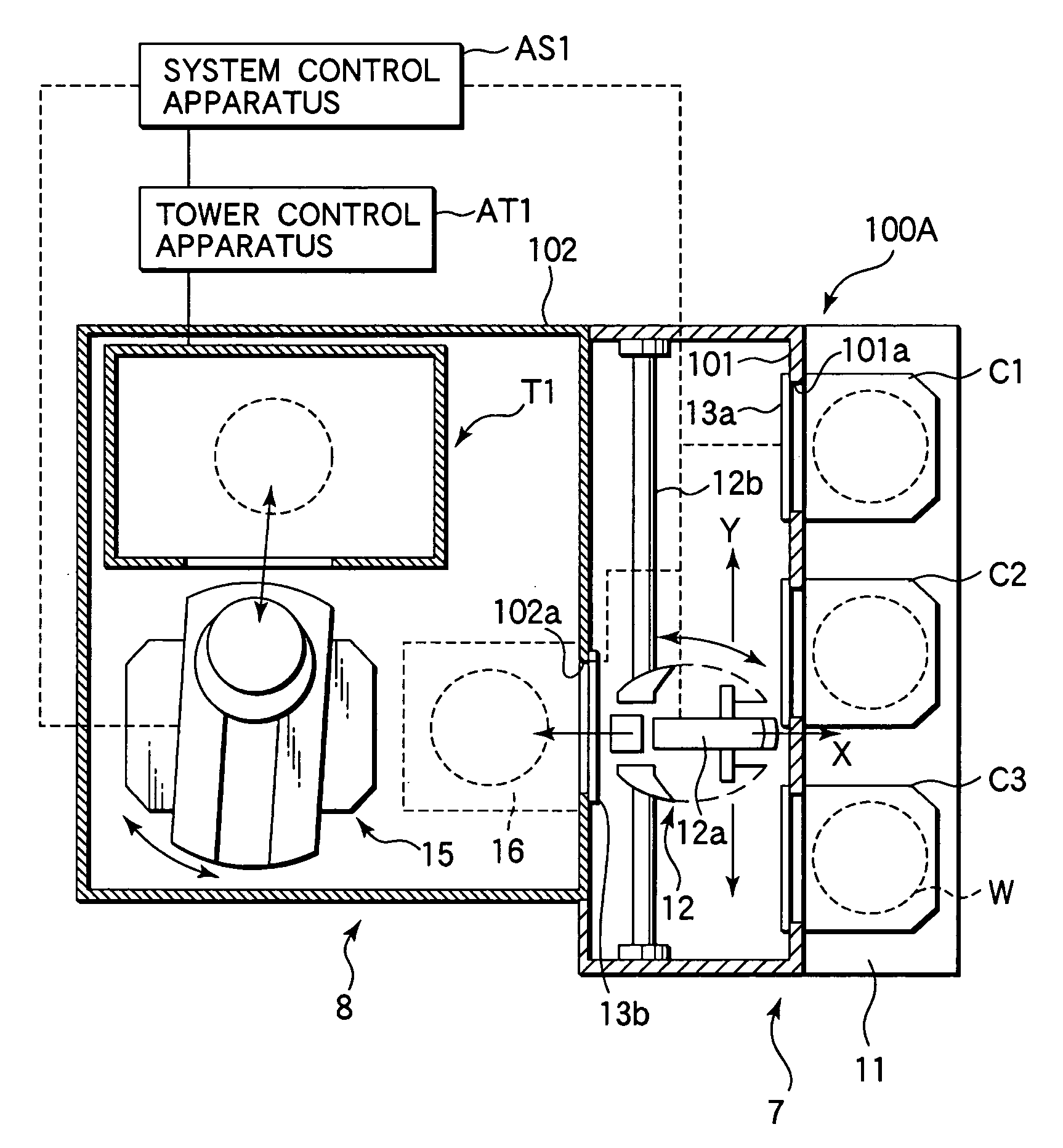
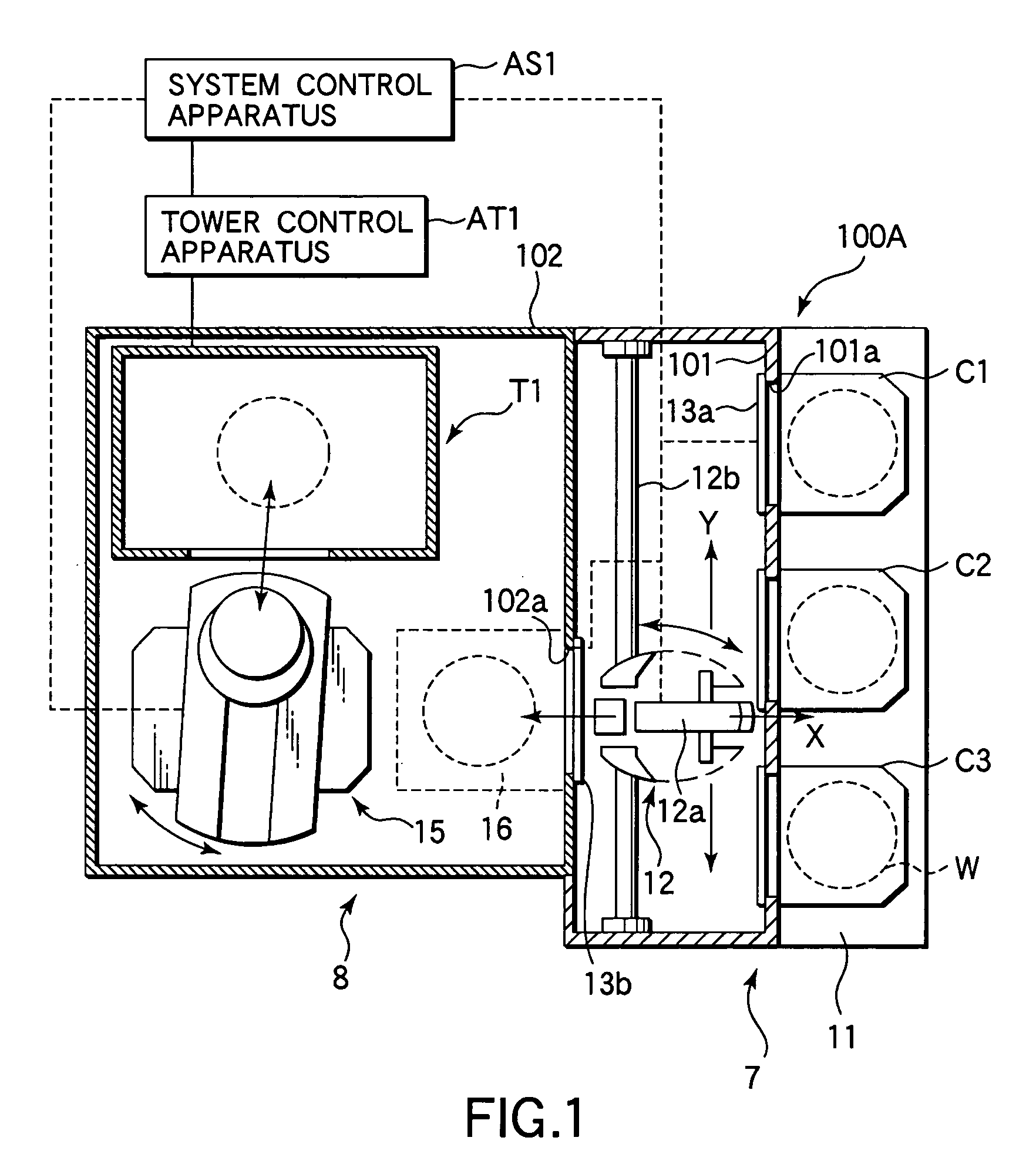
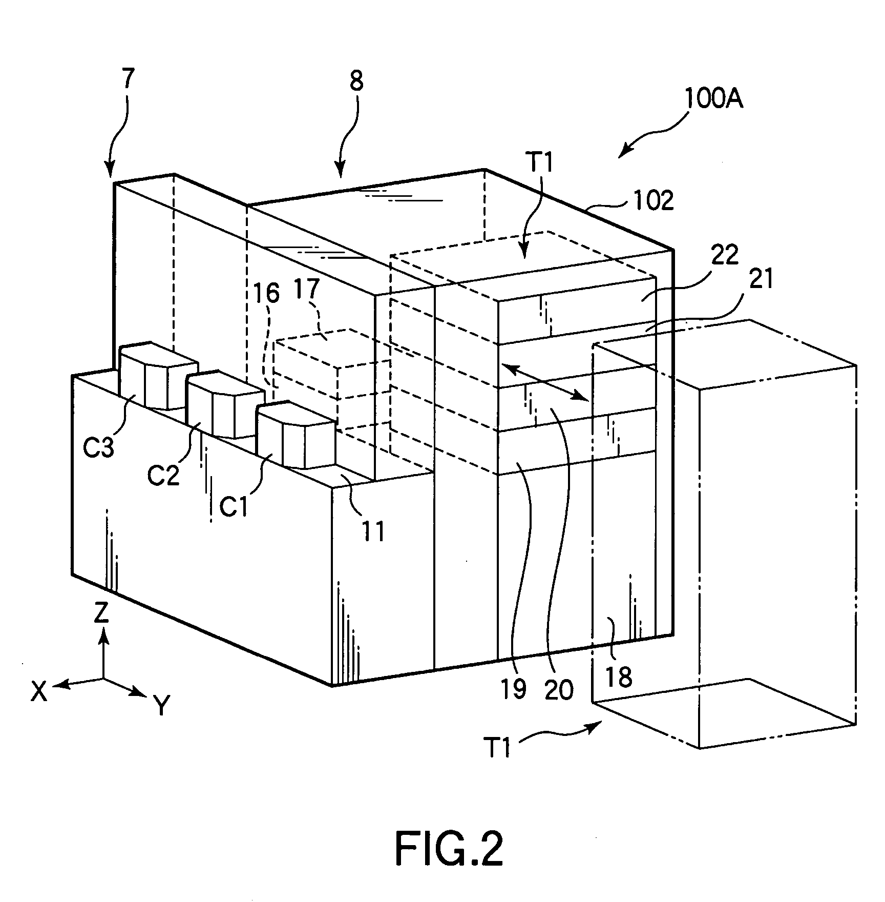
[0069]FIG. 1 is a horizontal cross sectional view schematically showing the construction of an SOD system 100A for forming an insulating film by an SOD method, and FIGS. 2 and 3 are an oblique view and a side view, respectively, each showing the construction of the SOD system 100A shown in FIG. 1.

[0070] The SOD system 100A comprises a process block 8 for applying a prescribed processing to a wafer W and a carrier block 7 for transferring the wafer W between a carrier C housing a prescribed number of wafers W and the process block 8.

[0071] The carrier block 7 includes a carrier table 11 on which a plurality of carriers, e.g., three carriers C1 to C3, can be disposed and a sub-transfer mechanism 12 for transferring the wafer W between the carriers C1 to C3 disposed on the carrier table 11 and the process block 8. The sub-transfer mechanism 12 is arranged within a housing ...


PUM


Abstract

An SOD system (100A) comprises a process block (8) for performing a prescribed processing so as to form an insulating film on a wafer W, a carrier block (7) for transferring the wafer W from the outside into the process block (8), a sub-transfer mechanism (12) for transferring the substrate W between the process block (8) and the carrier block (7), and a main transfer mechanism (15). A process tower (T1) prepared by stacking one upon the other a plurality of process units for performing a series of processing for forming an insulating film on the wafer W is arranged detachable from the process block (8).

Description

TECHNICAL FIELD [0001] The present invention relates to an insulating film-forming apparatus for forming an insulating film on a substrate such as a semiconductor wafer or an LCD substrate (a glass substrate for a liquid crystal display). BACKGROUND ART [0002] In the manufacturing process of a semiconductor device, an SOD (Spin on Dielectric) method is employed as one of the technologies for forming an insulating film (an interlayer insulating film) on a semiconductor wafer. In the SOD method, a coating film, i.e., a film formed by the coating method, is formed on a wafer by a spin coating method, followed by applying a chemical processing or a heat processing or the like to the coating film so as to form an insulating film. To be more specific, the surface of a wafer is coated first with a chemical liquid prepared by dispersing the material for forming the insulating film in a solvent, followed by evaporating the solvent from the coating film so as to dry the coating film. Then, a ...

Claims


Application Information

Patent Timeline
IPC IPC(8): B05B5/025H01L21/00
CPCH01L21/67017H01L21/6715H01L21/67754H01L21/67184H01L21/6719H01L21/67178
Inventor NISHIBAYASHI, TAKAHIRO
Owner TOKYO ELECTRON LTD
Learn More