
Semiconductor device and manufacturing method for the same

a technology of semiconductor devices and manufacturing methods, applied in the direction of semiconductor devices, basic electric elements, electrical appliances, etc., can solve the problems of difficult to gain a large drive current, uneven profile of implanted impurities, and irregular profile of important properties such as threshold voltage, on-resistance and the lik

Inactive Publication Date: 2006-01-19
SHARP KK
View PDF2 Cites 8 Cited by
  • Summary
  • Abstract
  • Description
  • Claims
  • Application Information

AI Technical Summary

Benefits of technology

[0030] a contact layer of the second conductive type which is formed within the body portion and of which the impurity concentration is higher than that of the body portion; and

Problems solved by technology

According to a method for forming an LDMOS in a self-aligning manner, which has been conventionally used, however, several problems arise as described below.
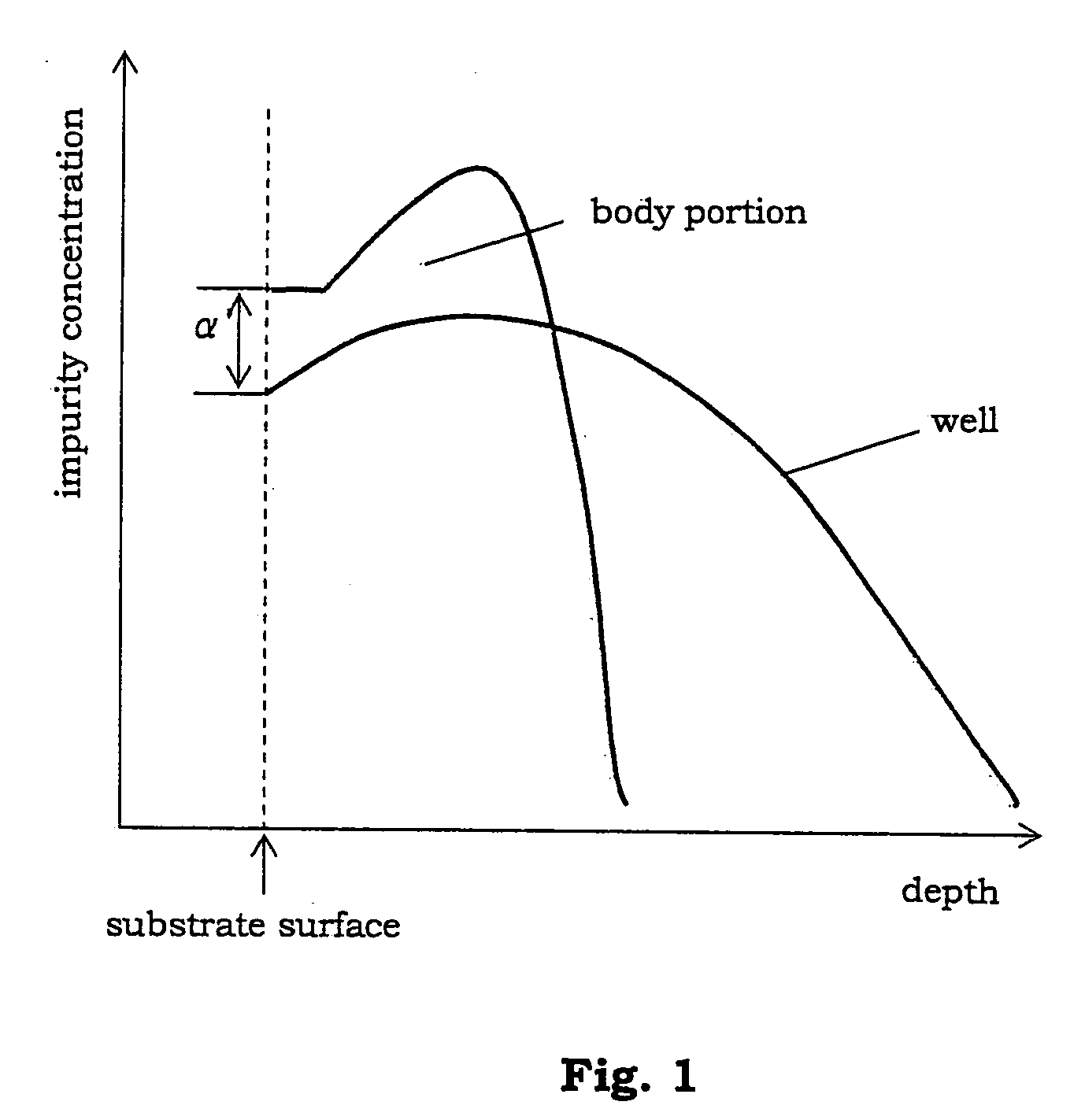
(1) A process for driving impurities into an area beneath the gate electrode by means of a heat treatment for a long period of time at a high temperature no lower than 1000° C. is necessary after the impurities have been implanted into the body portion, and therefore, a problem arises where the profile of the implanted impurities becomes uneven as a result of the redistribution due to the heat treatment.
As a result, the aforementioned method is a manufacturing method that important properties such as those in terms of a threshold voltage, an on-resistance and the like, tend to become irregular.
Therefore it is theoretically difficult to gain a large drive current, that is to say, to form an LDMOS of which the on-resistance is small.
(2) In a self-aligning system, the implantation energy is restricted by the thickness of the gate electrode which becomes a mask at the time of implantation in a body portion, and therefore, formation of a profile in the depth of direction is limited.
According to this method, however, a manufacturing method is used so as to include self alignment and thermal diffusion and therefore, the aforementioned problems (1) and (2) cannot be completely solved.

Method used


Image

  • Semiconductor device and manufacturing method for the same
  • Semiconductor device and manufacturing method for the same
  • Semiconductor device and manufacturing method for the same

Examples


embodiments

[0089] In the following, the invention is described in further detail in reference to the embodiments.

[0090] In the following embodiments, though N channel type LDMOS and VDMOS are cited, the invention is not limited to the N channel type LDMOS and VDMOS, and similar implementations are, or course, possible for P channel type LDMOS and VDMOS.

first embodiment

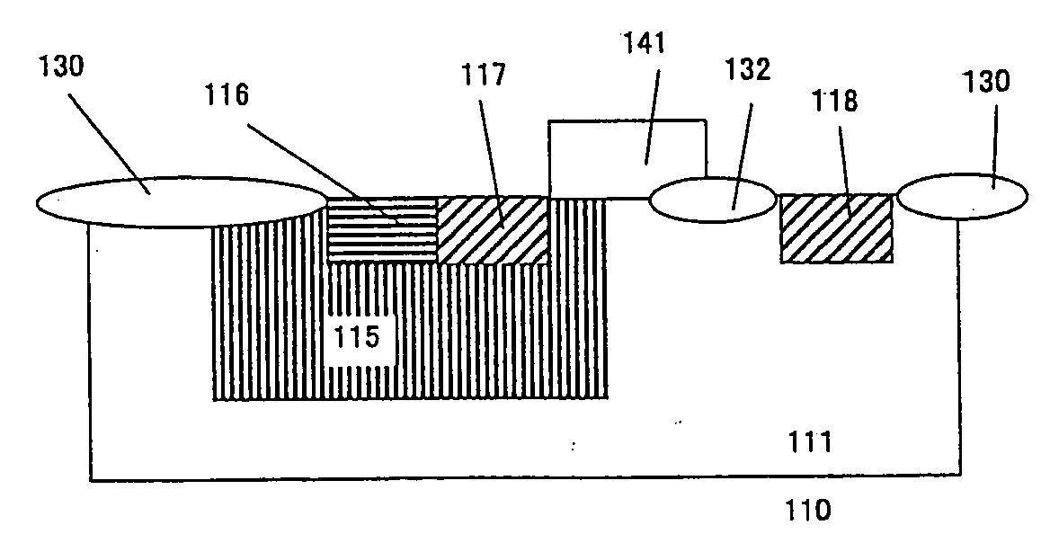
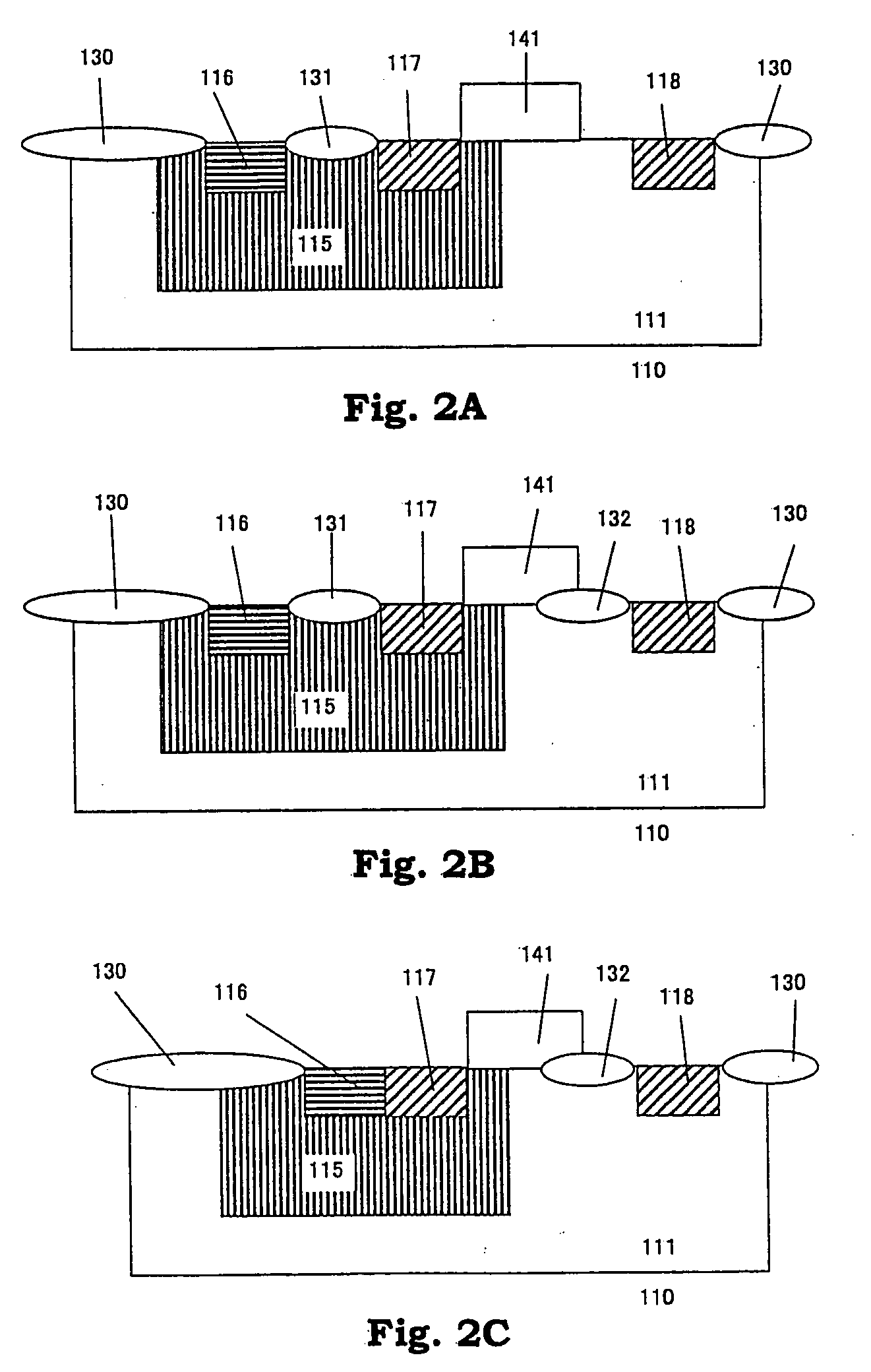
[0091]FIGS. 4A to 4M are cross sectional views schematically illustrating the steps in the fabrication of a semiconductor device according to a first embodiment.

Step (a)

[0092] First, as shown in FIG. 4A, 31p+ ions are implanted into a well formation region in a semiconductor substrate (Si substrate) 110, with an implantation amount of 1E13 ions / cm2 and an energy. of 400 KeV, and heat treatment at 1150° C. is carried out for 6 hours, so as to form an N well 111 having Xj up to 4 μm and a impurity concentration of 2E16 / cm3.

[0093] After that, a SiNx film is deposited, and the SiNx film is removed using a photoresist having an opening in an element isolation region. Next, the SiNx film is used as an oxide protective film in the transistor region, and a thermal oxidation process is carried out at 1050° C. for 2 hours, so as to form a thermal oxide film (field oxide film 130) of approximately 600 nm in the element isolation region. After this, the SiNx film is removed from the entiret...

second embodiment

[0108] The second embodiment provides a structure where a body portion is formed in an N well which becomes a drain region. The body portion may be formed in a P well, as shown in FIG. 4M′, in addition to the aforementioned structure.


PUM


Abstract

A manufacturing method for a semiconductor device, comprising the steps of: (a) forming a body portion of a DMOS by implanting impurity ions of a second conductive type into a predetermined region of a well of a first conductive type that has been formed in a main surface of a semiconductor substrate a plurality of times while changing an implantation amount or an implantation energy or both of them; (b) forming a gate dielectric film on the semiconductor substrate in a gate electrode formation region at least within the well, followed by a gate electrode on the gate dielectric film so as to cross an end of the body portion; (c) forming diffusion layers of the first conductive type on both sides of the gate electrode by implanting impurity ions of the first conductive type (provided that at least one of the diffusion layers is formed within the body portion); and (d) forming a contact layer of the second conductive type by implanting impurities of the second conductive type into the body portion with a impurity concentration higher than the impurity concentration in the body portion.

Description

CROSS-REFERENCE TO RELATED APPLICATION [0001] This application is related to Japanese application No. 2004-206340 filed on Jul. 13, 2004, the disclosure of which is incorporated by reference in its entirety. BACKGROUND OF THE INVENTION [0002] 1. Field of the Invention [0003] The invention relates to a semiconductor device and a manufacturing method for the same. In particular, the invention relates to a semiconductor device that includes a DMOS (Laterally Diffused MOS, which is hereinafter referred to as LDMOS, or vertically diffused MOS, which is hereinafter referred to as VDMOS) that can be utilized for a high voltage application such as one for a power supply, and to a manufacturing method for the same. [0004] 2. Description of the Related Art [0005] DMOSs are known as one type of high voltage transistors in integrated circuits that include a high voltage circuit such as one for a power supply. A body portion (channel portion) of such a DMOS has conventionally been manufactured i...

Claims


Application Information

Patent Timeline
Patent Type & Authority Applications(United States)
IPC IPC(8): H01L29/76
CPCH01L29/1095H01L29/66689H01L29/7816H01L29/7802H01L29/66719
Inventor YONEMOTO, HISASHINARUSE, KAZUSHIISHIKAWA, HIDEYUKIOKAYAMA, YASUHIKO
Owner SHARP KK
Learn More