Substrate for semiconductor device, method of manufacturing substrate for semiconductor device, substrate for electro-optical device, electro-optical device, and electronic apparatus

a semiconductor device and substrate technology, applied in the direction of semiconductor devices, electrical devices, basic electric elements, etc., can solve the problems of degrading the yield of manufacturing an electro-optical device, large substrate for a semiconductor device, and interlayer insulating film, etc., to achieve the effect of suppressing contact resistan

Inactive Publication Date: 2006-01-19
SEIKO EPSON CORP
View PDF2 Cites 7 Cited by
  • Summary
  • Abstract
  • Description
  • Claims
  • Application Information

AI Technical Summary

Benefits of technology

[0008] An advantage of the invention is that it provides a substrate for a semiconductor device that can suppress contact resistance in a stack contact, a method of manufacturing the substrate for a semiconductor device, a substrate for an electro-optical device that has such a substrate for a semiconductor device, an electro-optical device that has such a substrate for an electro-optical device, and an electronic apparatus.
[0009] According to a first aspect of the invention, a substrate for a semiconductor device includes a substrate, a thin film transistor that is provided on the substrate, a wiring line that is provided above the thin film transistor, an interlayer insulating film that electrically isolates the wiring line from at least a semiconductor layer of the thin film transistor, and a contact hole that has a first hole being cut in the interlayer insulating film and extending in a longitudinal direction as viewed from a substrate surface in plan view and a plurality of second holes passing through the interlayer insulating film from a bottom of the first hole to reach a surface of the semiconductor layer and being arranged in the longitudinal direction of the first hole, and that connects the wiring line to the semiconductor layer via the interlayer insulating film.
[0010] In accordance with the first aspect of the invention, on the substrate, the thin film transistor and the wiring line are electrically isolated from each other by a single or more-layered interlayer insulating film. In the interlayer insulating film, the contact hole that passes through the interlayer insulating film from a surface of the interlayer insulating film to reach the surface of the semiconductor layer of the thin film transistor is formed. As such, since the contact hole is formed in the interlayer insulating film, a wall portion of the interlayer insulating film that defines the contact hole is formed.
[0011] The contact hole has the first hole formed in the interlayer insulating film and the plurality of second holes formed in the bottom of the first hole. The first hole of the contact hole extends in the longitudinal direction along a direction of a channel width of the thin film transistor on the semiconductor layer and has a rectangular shape as viewed from the substrate surface in plan view. The first hole is not limited to the rectangular shape as viewed from the substrate surface in plan view, that is, the shape linearly extending in the longitudinal direction. For example, the first hole may be formed in a curved shape that has a first portion extending in the direction of the channel width of the thin film transistor and a second portion being curved to the linear portion. Further, a plurality of contact holes may be formed along the direction of the channel width of the thin film transistor.
[0012] Further, the plurality of second holes of the contact hole pass through the interlayer insulating film from the bottom of the first hole to reach the semiconductor layer. Further, the plurality of second holes are arranged along the longitudinal direction of the first hole as viewed from the substrate surface in plan view.
[0013] Then, in the contact hole, for example, the wiring line is continuously formed from the surface of the interlayer insulating film into the contact hole so as to cover an exposed surface of the semiconductor layer in the contact hole. In this case, a stack contact may be formed with a part of the wiring line formed in the contact hole. A source or a drain of the thin film transistor is electrically connected to the wiring line via the stack contact. Here, one of the source and the drain of the thin film transistor is connected to the wiring line via the stack contact according to the first aspect of the invention. Alternatively, both the source and the drain of the thin film transistor may be connected to the wiring line via the stack contact according to the first aspect of the invention.

Problems solved by technology

In this case, however, when the driving circuit is reduced in size by narrowing the pitch of the wiring line, an interlayer insulating film that electrically isolates the wiring line from an additional conductive layer formed above the wiring line may be cracked.
Thus, there may be a problem in that the yield in manufacturing an electro-optical device is degraded.
However, if the distances of the contact holes are widened, the thin film transistor becomes large, and thus the substrate for a semiconductor device also becomes large.
Accordingly, the disconnection failure may occur.
Here, when a rubbing process is performed, if the step generated in the surface of the alignment film is large, the surface of the alignment film may be damaged, the film may be removed.

Method used


Image

  • Substrate for semiconductor device, method of manufacturing substrate for semiconductor device, substrate for electro-optical device, electro-optical device, and electronic apparatus
  • Substrate for semiconductor device, method of manufacturing substrate for semiconductor device, substrate for electro-optical device, electro-optical device, and electronic apparatus
  • Substrate for semiconductor device, method of manufacturing substrate for semiconductor device, substrate for electro-optical device, electro-optical device, and electronic apparatus

Examples


Embodiment Construction

[0090] Hereinafter, an embodiment of the invention will be described with reference to the drawings. In the embodiment described below, an electro-optical device of the invention is applied to a liquid crystal device.

1: Overall Configuration of Electro-Optical Device

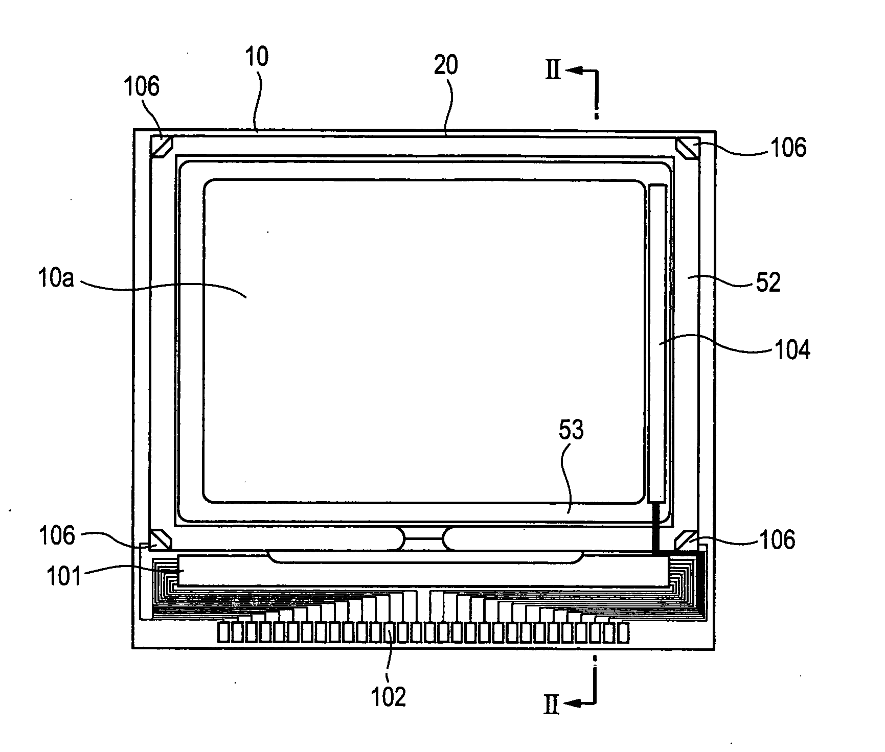
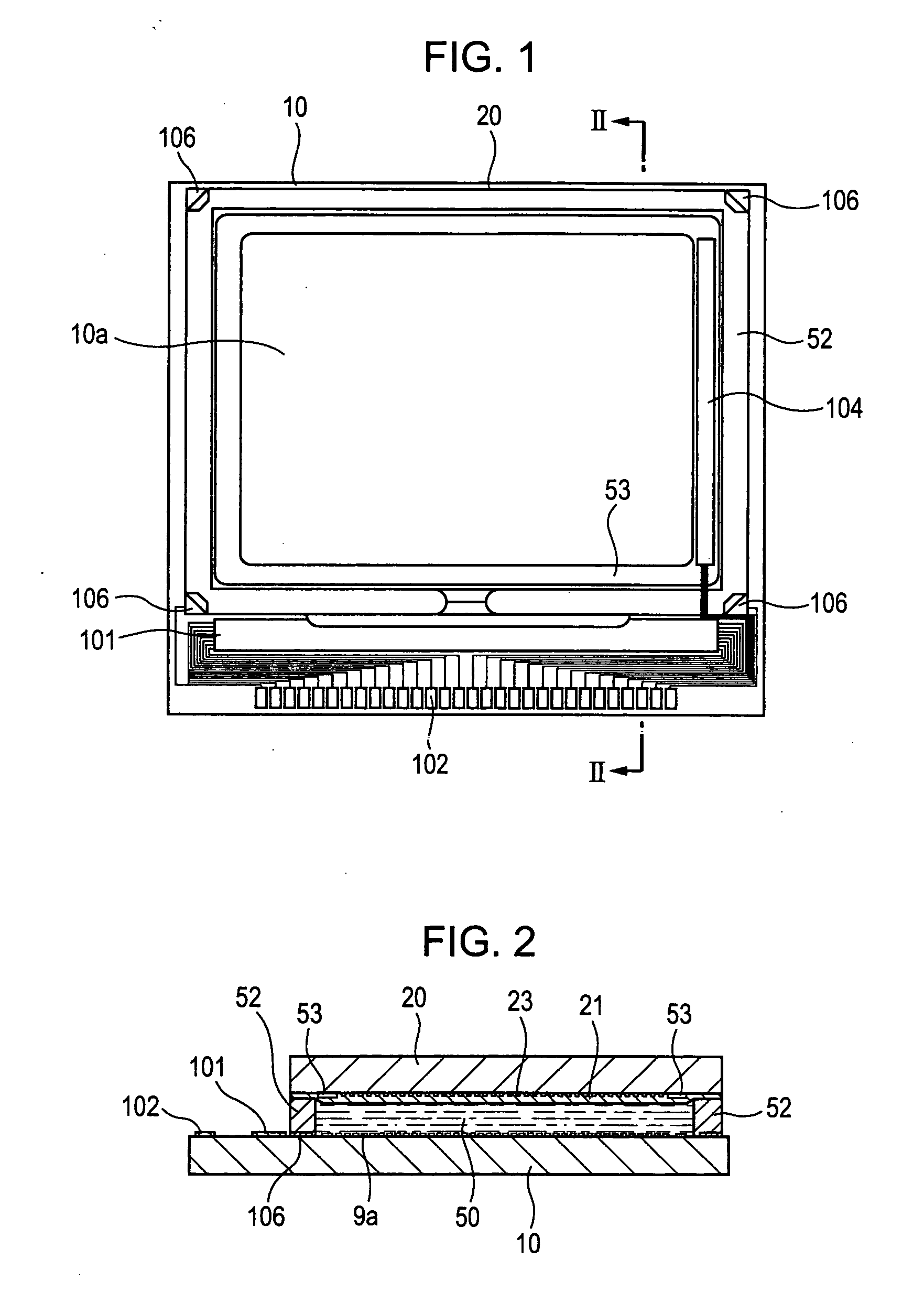
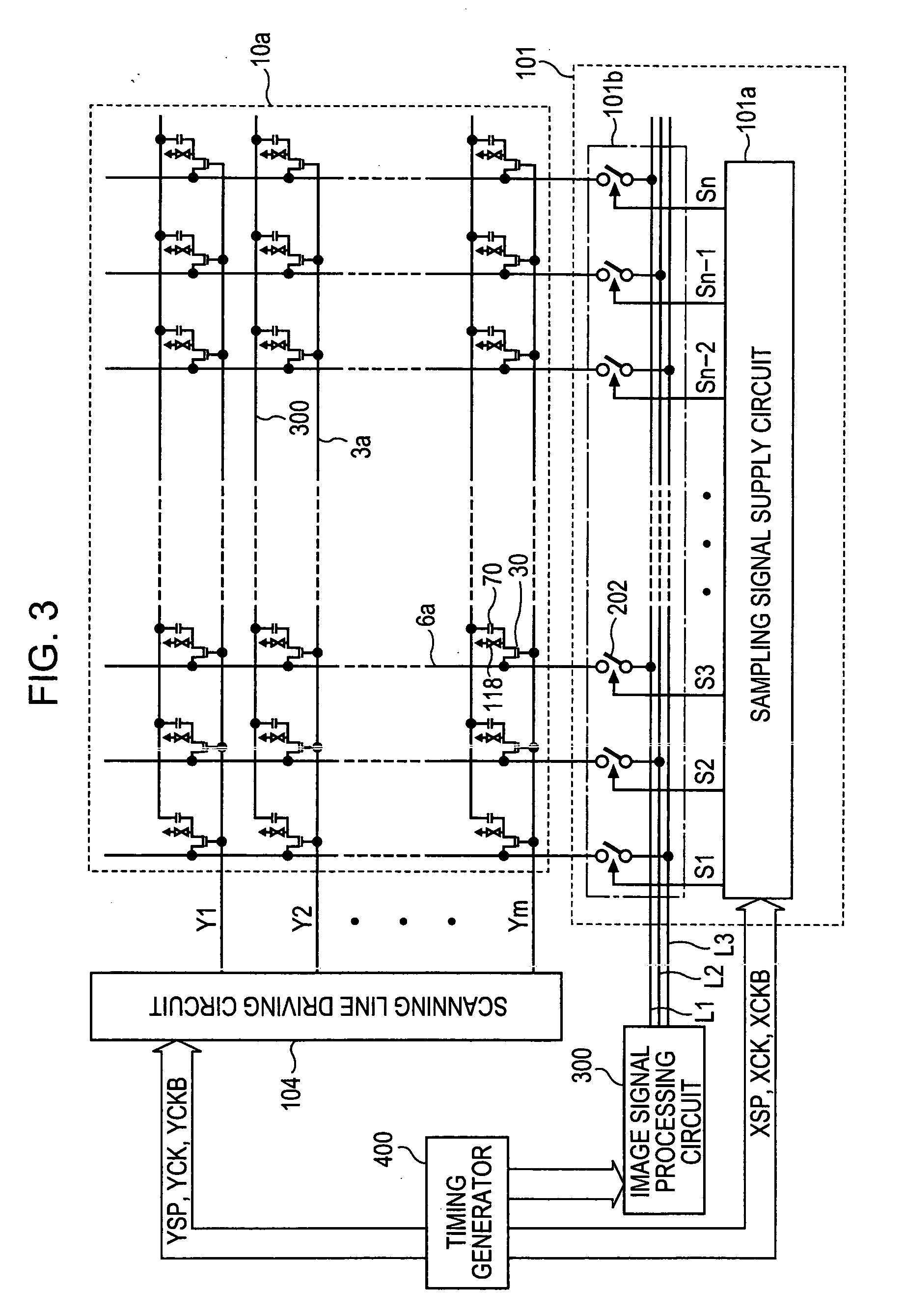
[0091] First, the overall configuration of an electro-optical device of the invention will be described with reference to FIGS. 1 to 3. FIG. 1 is a plan view of an electro-optical device as viewed from a counter substrate, together with a TFT array substrate and respective constituents formed thereon. FIG. 2 is a cross-sectional view taken along the line II-II of FIG. 1. Further, FIG. 3 is a block diagram showing an electrical configuration of an electro-optical device. Here, as an example of an electro-optical device, a TFT active matrix driving-type liquid crystal device having built-in driving circuits is used.

[0092] Referring to FIGS. 1 and 2, in the electro-optical device according to the present embodiment, a T...


PUM


Abstract

A substrate for a semiconductor device includes a substrate, a thin film transistor that is provided on the substrate, a wiring line that is provided above the thin film transistor, an interlayer insulating film that electrically isolates the wiring line from at least a semiconductor layer of the thin film transistor, and a contact hole that has a first hole being cut in the interlayer insulating film and extending in a longitudinal direction in plan view on a substrate surface and a plurality of second holes passing through the interlayer insulating film from a bottom of the first hole to reach a surface of the semiconductor layer and being arranged in the longitudinal direction of the first hole. The connect hole connects the wiring line to the semiconductor layer via the interlayer insulating film.

Description

BACKGROUND OF THE INVENTION [0001] 1. Technical Field [0002] The present invention relates to a substrate for a semiconductor device in which a contact hole is provided in a laminated structure on the substrate and that is used for an electro-optical device, such as a liquid crystal device or the like, to a method of manufacturing the substrate for a semiconductor device, to a substrate for an electro-optical device that has such a substrate for a semiconductor device, to an electro-optical device that has such a substrate for an electro-optical device, and to an electronic apparatus, such as a projector, or the like. [0003] 2. Related Art [0004] In Japanese Unexamined Patent Application Publication No. 8-227939, a substrate for a semiconductor device in which a multi-layered wiring line is formed using a stack contact is disclosed. Further, in Japanese Unexamined Patent Application Publication No. 2002-108244, an electro-optical device that has such a substrate for a semiconductor ...

Claims


Application Information

Patent Timeline
Patent Type & Authority Applications(United States)
IPC IPC(8): H01L27/12H01L21/84
CPCH01L27/12H01L27/1248H01L27/124H01L21/28H01L21/3205
Inventor MORIWAKI, MINORU
Owner SEIKO EPSON CORP
Why Eureka
Try Eureka