

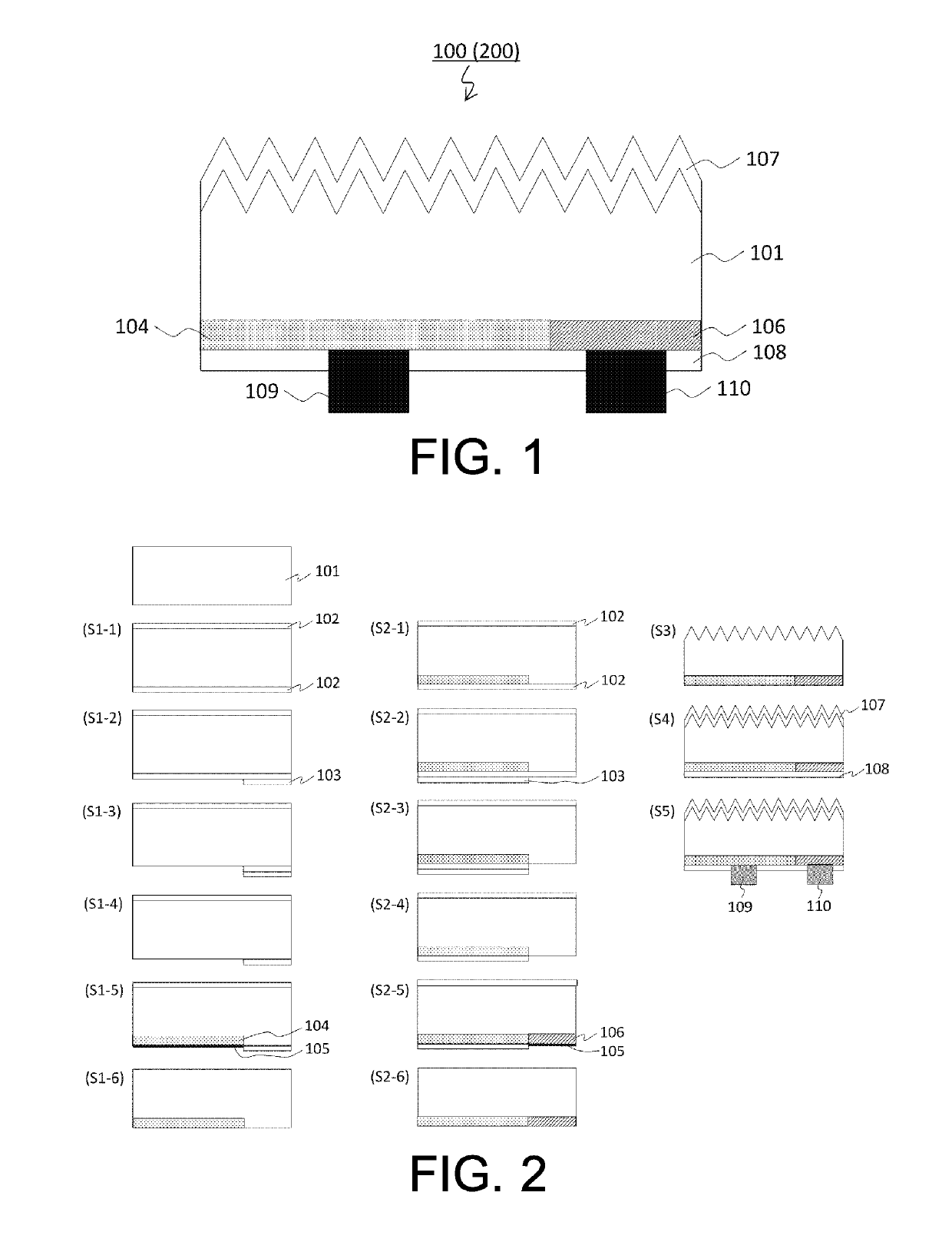
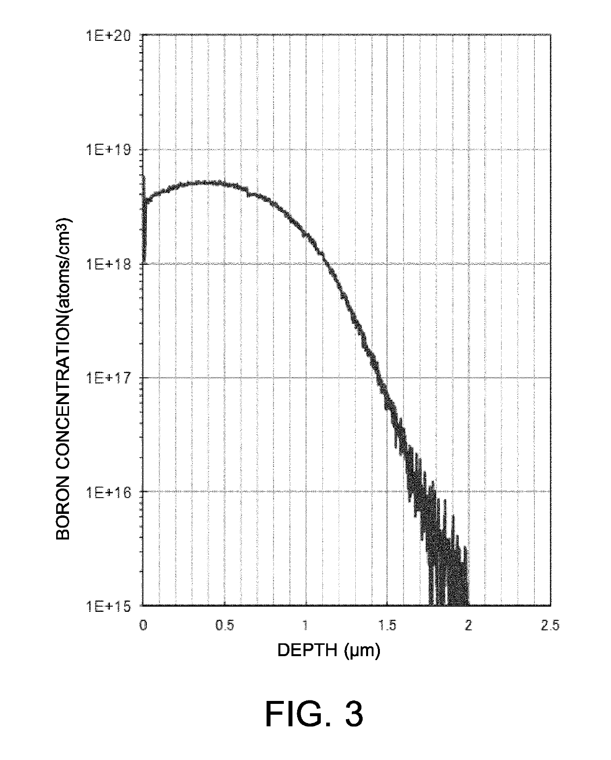
High efficiency back contact type solar cell, solar cell module, and photovoltaic power generation system
a solar cell and back contact technology, applied in the direction of climate sustainability, sustainable manufacturing/processing, semiconductor devices, etc., can solve the problems of deteriorating conversion efficiency, increasing current, and difficulty in reducing contact resistance in sufficient amounts, so as to achieve favorable conversion efficiency and reduce current density , the effect of small reverse saturation current density
- Summary
- Abstract
- Description
- Claims
- Application Information
AI Technical Summary
Benefits of technology
Problems solved by technology
Method used
Image

Examples
example 1
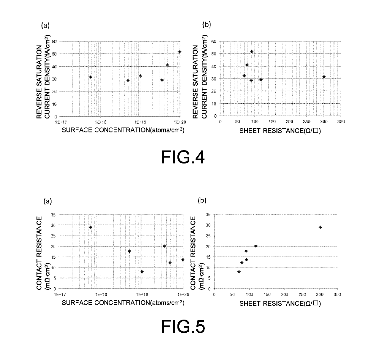
[0066]Example 1 is the case of extending the thermal oxidation time to 90 minutes in Comparative Example 1.
[0067]The substrate formed with the emitter layer as described above was set in an oxygen atmosphere and thermally oxidized at a temperature of 1000° C. for 90 minutes, to form a silicon oxide layer on each surface of the substrate with a thickness of 80 nm. By the thermal treatment at this time, boron diffused in the emitter layer was re-diffused. The diffusion profile of boron in the emitter layer after the re-diffusion was measured by SIMS, resulting in that the surface concentration was 5.0×10¹⁹ atms / cm3, the maximum concentration was 7×10¹⁹ atms / cm3, the depth at which the maximum concentration was obtained was 0.1 μm, and the diffusion depth was 1.0 μm. The sheet resistance of the emitter layer was about 60 Ω / □.
example 2
[0068]Example 2 is the case of extending the thermal oxidation time to 120 minutes in Comparative Example 1.
[0069]The substrate formed with the emitter layer as described above was set in an oxygen atmosphere and thermally oxidized at a temperature of 1000° C. for 120 minutes, to form a silicon oxide layer on each surface of the substrate with a thickness of 100 nm. By the thermal treatment at this time, boron diffused in the emitter layer was re-diffused. The diffusion profile of boron in the emitter layer after the re-diffusion was measured by SIMS, resulting in that the surface concentration was 1.0×10¹⁹ atms / cm3, the maximum concentration was 1.2×10¹⁹ atms / cm3, the depth at which the maximum concentration was obtained was 0.4 μm, and the diffusion depth was 2.0 μm. The sheet resistance of the emitter layer was about 70 Ω / □.
example 3
[0070]Example 3 is the case of extending the thermal oxidation time to 180 minutes in Comparative Example 1.
[0071]The substrate formed with the emitter layer as described above was set in an oxygen atmosphere and thermally oxidized at a temperature of 1000° C. for 180 minutes, to form a silicon oxide layer on each surface of the substrate with a thickness of 130 nm. By the thermal treatment at this time, boron diffused in the emitter layer was re-diffused. The diffusion profile of boron in the emitter layer after the re-diffusion was measured by SIMS, resulting in that the surface concentration was 5.0×10¹⁸ atms / cm3, the maximum concentration was 8.0×10¹⁸ atms / cm3, the depth at which the maximum concentration was obtained was 0.7 μm, and the diffusion depth was 2.3 μm. The sheet resistance of the emitter layer was about 90 Ω / □.
PUM
 Abstract
Description
Claims
Application Information