CMOS image sensor and method for fabricating the same

a metal oxide semiconductor and image sensor technology, applied in the field of image sensors, can solve the problems of consuming a large amount of power, complicated driving method, and inability to easily form one-chip circuits, etc., and achieve the effect of enhancing device integration and reducing the radius of a curvature of a micro-lens

Inactive Publication Date: 2006-01-19
DONGBU ELECTRONICS CO LTD
View PDF5 Cites 22 Cited by
  • Summary
  • Abstract
  • Description
  • Claims
  • Application Information

AI Technical Summary

Benefits of technology

[0014] An object of the present invention is to provide a complementary metal-oxide semiconductor (CMOS) image sensor and a method for fabricating the same, which can reduce a radius of a curvature of a micro-lens, thereby enhancing integration of the device.

Problems solved by technology

However, the CCD is disadvantageous in that the driving method is complicated and consumes a large amount of power, and the fabrication process is complicated having too many mask process steps.
Furthermore, a one-chip circuit cannot be easily formed because the signal processing circuit cannot be realized in the CCD chip.
However, the reflow process is difficult to control, thereby causing problems in fabricating the micro-lens in a dome shape.
However, the photoresist cannot be formed thinner than a predetermined thickness.
Thus, there are limitations in reducing the radius of the curvature of the micro-lens, thereby causing difficulty in the integration of the device.

Method used


Image

  • CMOS image sensor and method for fabricating the same
  • CMOS image sensor and method for fabricating the same
  • CMOS image sensor and method for fabricating the same

Examples


Embodiment Construction

[0024] Reference will now be made in detail to the preferred embodiments of the present invention, examples of which are illustrated in the accompanying drawings. Wherever possible, the same reference numbers will be used throughout the drawings to refer to the same or like parts.

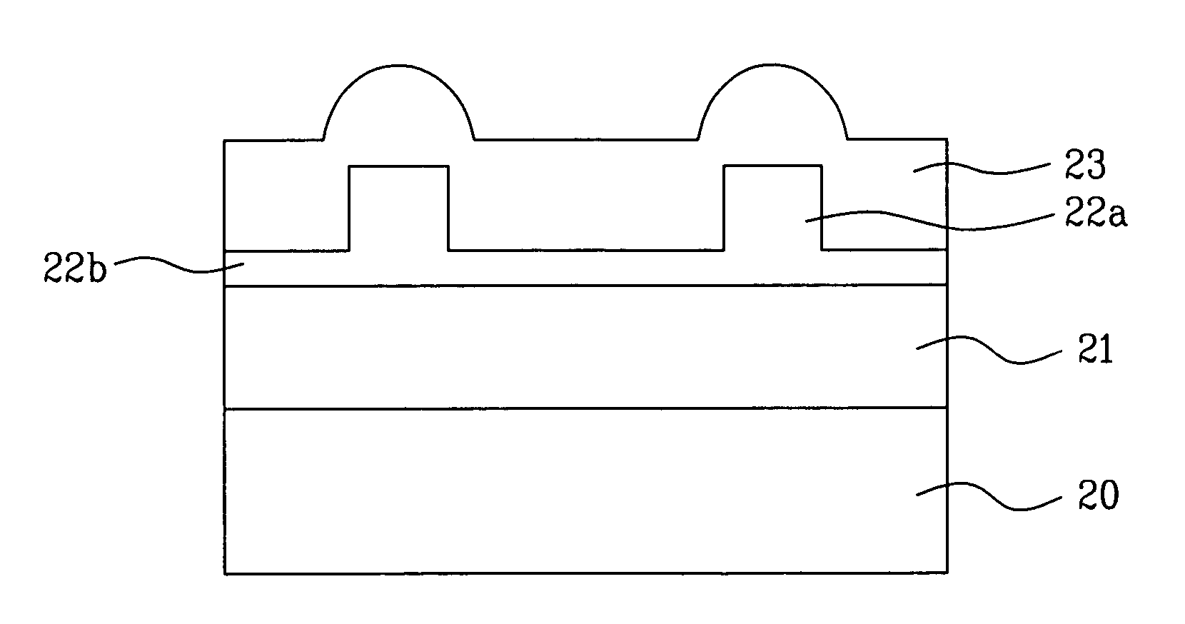
[0025]FIG. 3 illustrates a structure of a CMOS image sensor according to the present invention. Herein, a pad insulating layer 21 is formed on a sub-layer 20 having a photodiode and various transistors formed thereon. Then, a micro-lens 24 is formed on the pad insulating layer 21. The micro-lens 24 includes a first insulating layer 22 having an uneven surface, and a second insulating layer 23 formed in a dome shape by covering upper and side surfaces of projected portions of the uneven surface.

[0026] Herein, it is preferable that the first insulating layer 22 is formed of a nitride layer, and that the second insulating layer 23 is formed of an oxide layer. In addition, a planarization layer 25 is formed o...


PUM


Abstract

A complementary metal-oxide semiconductor (CMOS) image sensor and a method for fabricating the same are disclosed. The image sensor includes a sub-layer having a photodiode and a plurality of transistors formed thereon, a pad insulating layer formed on the sub-layer, a micro-lens formed on the pad insulating layer, the micro-lens including a first insulating layer having an uneven surface and a second insulating layer covering upper and side surfaces of a projected portion of the first insulating layer to form a dome shape, and a planarization layer formed on the micro-lens, and a color filter formed on the planarization layer.

Description

[0001] This application claims the benefit of the Korean Patent Application No. 10-2004-0055106, filed on Jul. 15, 2004, which is hereby incorporated by reference as if fully set forth herein. BACKGROUND OF THE INVENTION [0002] 1. Field of the Invention [0003] The present invention relates to an image sensor, and more particularly, to a complementary metal-oxide semiconductor (CMOS) image sensor and a method for fabricating the same. Although the present invention is suitable for a wide scope of applications, it is particularly suitable for enhancing a degree of integration of the device. [0004] 2. Discussion of the Related Art [0005] Generally, an image sensor is a semiconductor device, which converts an optic image to an electric signal. More specifically, a charge coupled device (CCD) is a device having a plurality of metal-oxide-metal (MOS) capacitors each formed within a proximate range from one another, and wherein a carrier electric charge is stored in and transmitted to each...

Claims


Application Information

Patent Timeline
Patent Type & Authority Applications(United States)
IPC IPC(8): H01L31/0232H01L31/062H01L27/14H01L33/00H01L27/146
CPCH01L21/31116H01L27/14685H01L27/14627H01L27/146H01L31/10
Inventor KIM, IN SU
Owner DONGBU ELECTRONICS CO LTD
Why Eureka
Try Eureka