Flip-chip packaged SMD-type LED with antistatic function and having no wire bonding

a technology of anti-static function and packaging, which is applied in the direction of semiconductor devices, semiconductor/solid-state device details, electrical apparatus, etc., can solve the problems of reducing the yield rate, reducing the thickness of the light-emitting device, and ensuring upward light loss, etc., to achieve good static control

Active Publication Date: 2006-01-19
EPISTAR CORP
View PDF3 Cites 32 Cited by
  • Summary
  • Abstract
  • Description
  • Claims
  • Application Information

AI Technical Summary

Benefits of technology

[0014] It is a primary object of the present invention to provide a flip-chip packaged SMD-type LED with antistatic function and having no wire bonding that is packaged in flip chip packages so as to make the p-type electrode and the n-type electrode locate at the same side. An electrostatic protection device and a high electrical and heat conductive component are connected with the light emitting diode so as to avoid the problem of wire bonding and have a good static control effect.
[0015] In order to achieve above object, a flip-chip packaged SMD-type LED with antistatic function and having no wire bonding is provided. The invention includes a light emitting diode packaged in flip chip packages, an electrostatic protection device such as a transient voltage suppressor (TVS) or a Zener diode connected with the light emitting diode. Then the electrostatic protection device is attached with a substrate to form a flip-chip packaged SMD-type LED. The light emitting diode is connected to a lead frame of the substrate by a high electrical and heat conductive component thus the invention needs no wire bonding. Due to the electrostatic protection device, the invention has static control effect.

Problems solved by technology

Thus the upward light-emitting surface of the devices packaged by conventional methods is shielded by electrodes, and lead to a certain upward light loss.
Thus this also causes the reduction of the yield rate.
Due to the need of wire bonding, the thickness of the light-emitting device can't be dramatically reduced.

Method used


Image

  • Flip-chip packaged SMD-type LED with antistatic function and having no wire bonding
  • Flip-chip packaged SMD-type LED with antistatic function and having no wire bonding
  • Flip-chip packaged SMD-type LED with antistatic function and having no wire bonding

Examples


Embodiment Construction

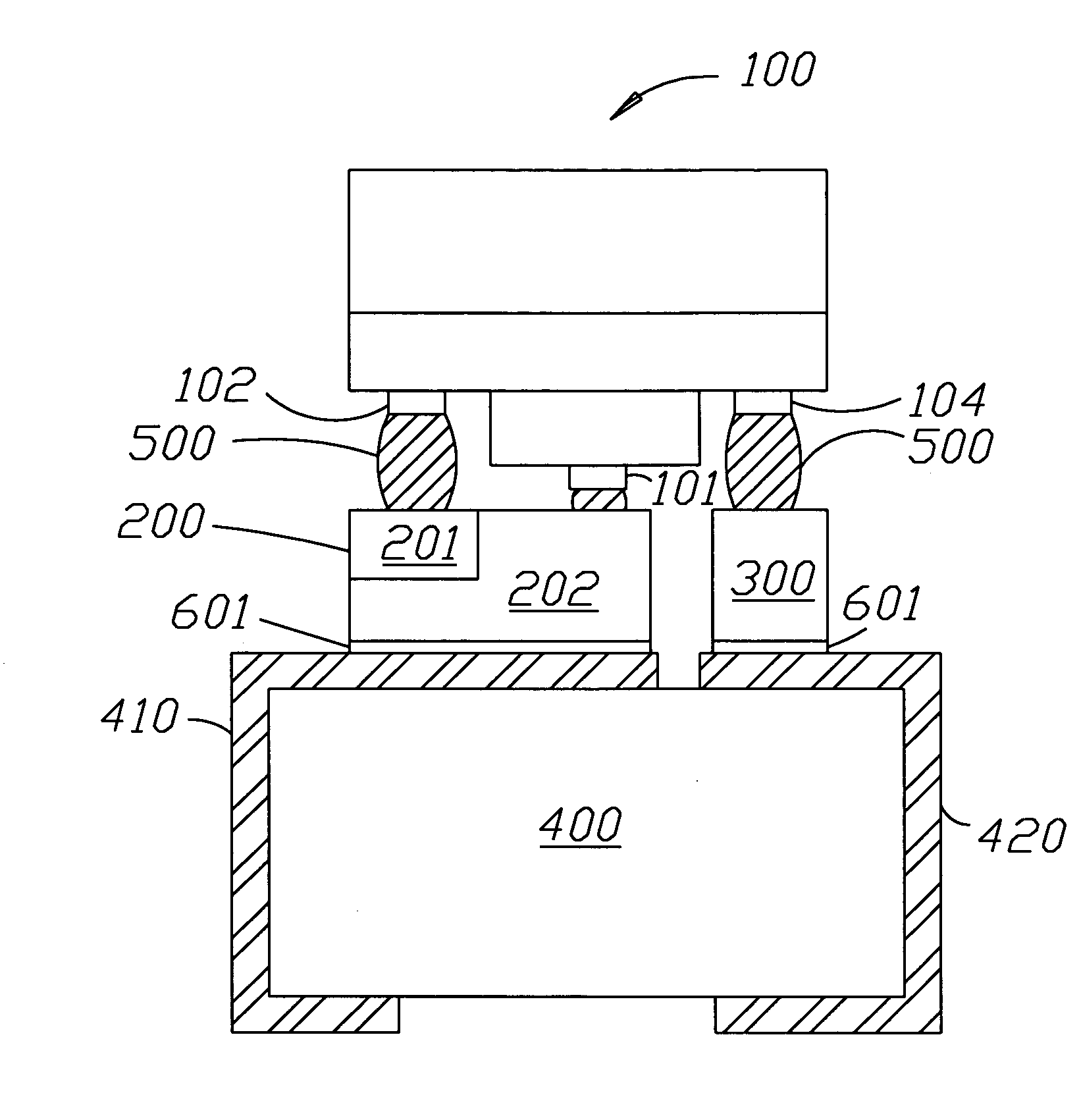
[0025] The present invention features on that an electrostatic protection device with static control effect and avoid the wire bonding problems of conventional SMD-type light emitting diode.

[0026] Refer to FIG. 4, a better embodiment of the present invention is disclosed. A SMD-type LED of the present invention includes a chip of gallium nitride-based III-V group compound semiconductor light-emitting device 100, an electrostatic protection device 200 such as a Zener diode, a high electrical and heat conductive component 300 and a high electrical and heat conductive base substrate 400 having a first lead frame 410 and a second lead frame 420. In this embodiment, the chip of gallium nitride-based III-V group compound semiconductor light-emitting device 100 includes a second p-type electrode 101, and two n-type electrodes apart from each other—a second n-type electrode 102 and a third n-type electrode 104, all located at the same side. The electrostatic protection device 200 having a ...


PUM


Abstract

A flip-chip packaged SMD-type (surface-mount device) light emitting diode is provided. The light emitting diode chip is packaged in flip chip packages and is connected with an electrostatic protection device such as a transient voltage suppressor (TVS) or a Zener diode. The electrostatic protection device is attached with a substrate so as to form a flip-chip packaged SMD-type light emitting diode. The light emitting diode chip is connected to a lead frame of the substrate by a high electrical and heat conductive component thus the device needs no wire bonding. Due to the electrostatic protection device, the device has static control effect.

Description

BACKGROUND OF THE INVENTION [0001] The present invention relates to a flip-chip packaged SMD-type (surface-mount device) light emitting diode, especially to a light emitting diode having an electrostatic protection device with function of standing electrostatic discharge (ESD) and without the need of wire bonding. [0002] Light emitting diode (LED) is a fine solid-state light source made of semiconductor material. The device that turns electricity into light features on the compact structure, long lifetime, low driving voltage, fast response, and good shock resistance. It can also be applied in various appliances with light weight and compact design and is quite popular in our daily lives. [0003] According to wavelength, LED is divided into visible LED and invisible LED. The visible LED is used for display. Moreover, the general LED and high brightness LED are differentiated by the brightness—one candle. The former is applied to indoor display systems while the later is suitable for ...

Claims


Application Information

Patent Timeline
Patent Type & Authority Applications(United States)
IPC IPC(8): H01L23/48H01L25/16H01L33/48
CPCH01L25/167H01L2224/48247H01L2924/3025H01L2224/48227H01L2224/48091H01L2924/00014H01L2924/00
Inventor LAI, MU-JEN
Owner EPISTAR CORP
Why Eureka
Try Eureka