Charge pump circuit

Active Publication Date: 2006-01-19
ABLIC INC
View PDF6 Cites 6 Cited by
  • Summary
  • Abstract
  • Description
  • Claims
  • Application Information

AI Technical Summary

Benefits of technology

[0011] To solve the conventional problems as described above, it is therefore an object of the present invention to minimize the reduction in the output voltage of the boosting charge pump circuit by suppressing the back-gate effect on the MOS transistors, and allow a high output voltage to be obtained from the boosting charge pump circuit with a small number of stages.
[0012] To suppress the back-gate effect exerted on a MOS transistor, a charge pump circuit according to the present invention is constituted such that a potential in the well of the MOS transistor is given by a source-well parasitic diode and by a drain-well parasitic diode.
[0017] The boosting charge pump circuit according to the present invention has an effect of suppressing the back-gate effect on the MOS transistor by giving the potential in the well of the MOS transistor as described above, thereby allowing a high output voltage to be obtained from the boosting circuit with a small number of stages.
[0018] By switching the potential in the well of the MOS transistor by using the second MOS transistor, a backflow due to a leakage current can be suppressed.

Problems solved by technology

The conventional charge pump circuit has had a problem in that the threshold voltages increase due to the back-gate effect exerted on the MOS transistors and the output voltage is thereby lowered.
In other words, there has been a problem in that the number of stages in the boosting charge pump circuit should be increased in order to obtain a desired output voltage.

Method used


Image

  • Charge pump circuit
  • Charge pump circuit
  • Charge pump circuit

Examples


embodiment 1

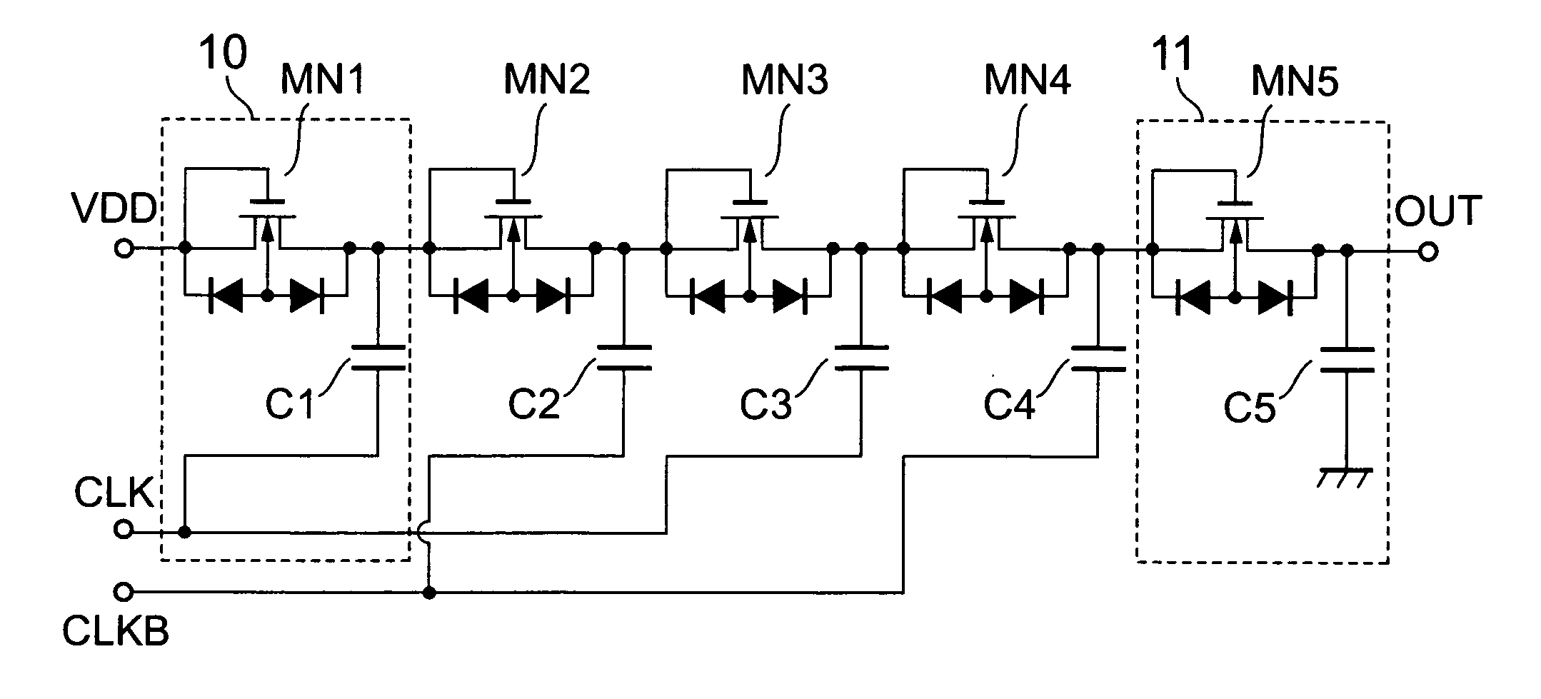
[0036] Referring now to the drawings, the embodiments of the present invention will be described herein below. FIG. 1 shows a boosting charge bump circuit according to a first embodiment of the present invention.

[0037] The respective voltages applied to the n-channel MOS transistors MN1 to MN5, the capacitors C1 to C5, the VDD terminal, the CLK terminal, and the CLKB terminal are equal to those applied in the conventional embodiment. The difference between the embodiments of the present invention and conventional embodiments is that the well potentials of the MOS transistors MN1 to MN5 are given by parasitic diodes. The parasitic diodes exist between the respective wells of the n-channel MOS transistors MN1 to MN5 and the respective sources and drains thereof. Specifically, a unit boosting circuit 10 is composed of an n-channel MOS transistor using the gate and drain thereof connected to each other as an input terminal and using the source thereof as an output terminal, and parasit...

embodiment 2

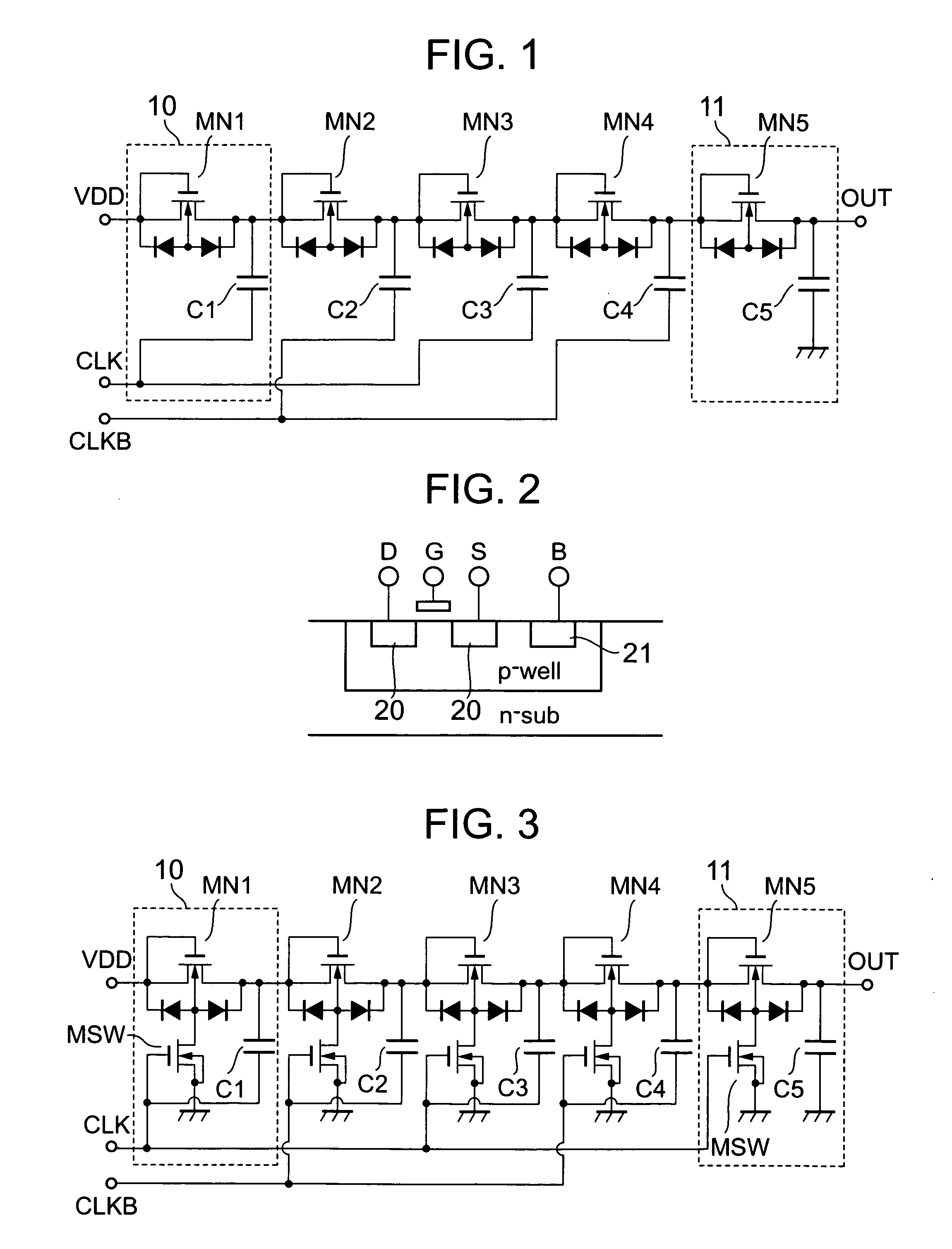
[0048]FIG. 3 shows a second embodiment of the boosting charge pump circuit according to the present invention. The voltages applied respectively to the n-channel MOS transistors MN1 to MN5, the capacitors C1 to C5, the VDD terminal, the CLK terminal, and the CLKB terminal are equal to those applied in the conventional embodiment. The difference between the embodiments of the present invention and conventional embodiments is that the well potential of each of the MOS transistors MN1 to MN5 is connected to the reference voltage (GND) via a switch transistor MSW. The switch transistor MSW has the gate connected to the CLK or CLKD terminal.

[0049] Specifically, the unit boosting circuit 10 is composed of an n-channel MOS transistor using the gate and drain thereof connected to each other as an input terminal and using the source thereof as an output terminal, a capacitor connected to the output terminal, and an n-channel MOS transistor having the drain thereof connected to the well of t...

embodiment 3

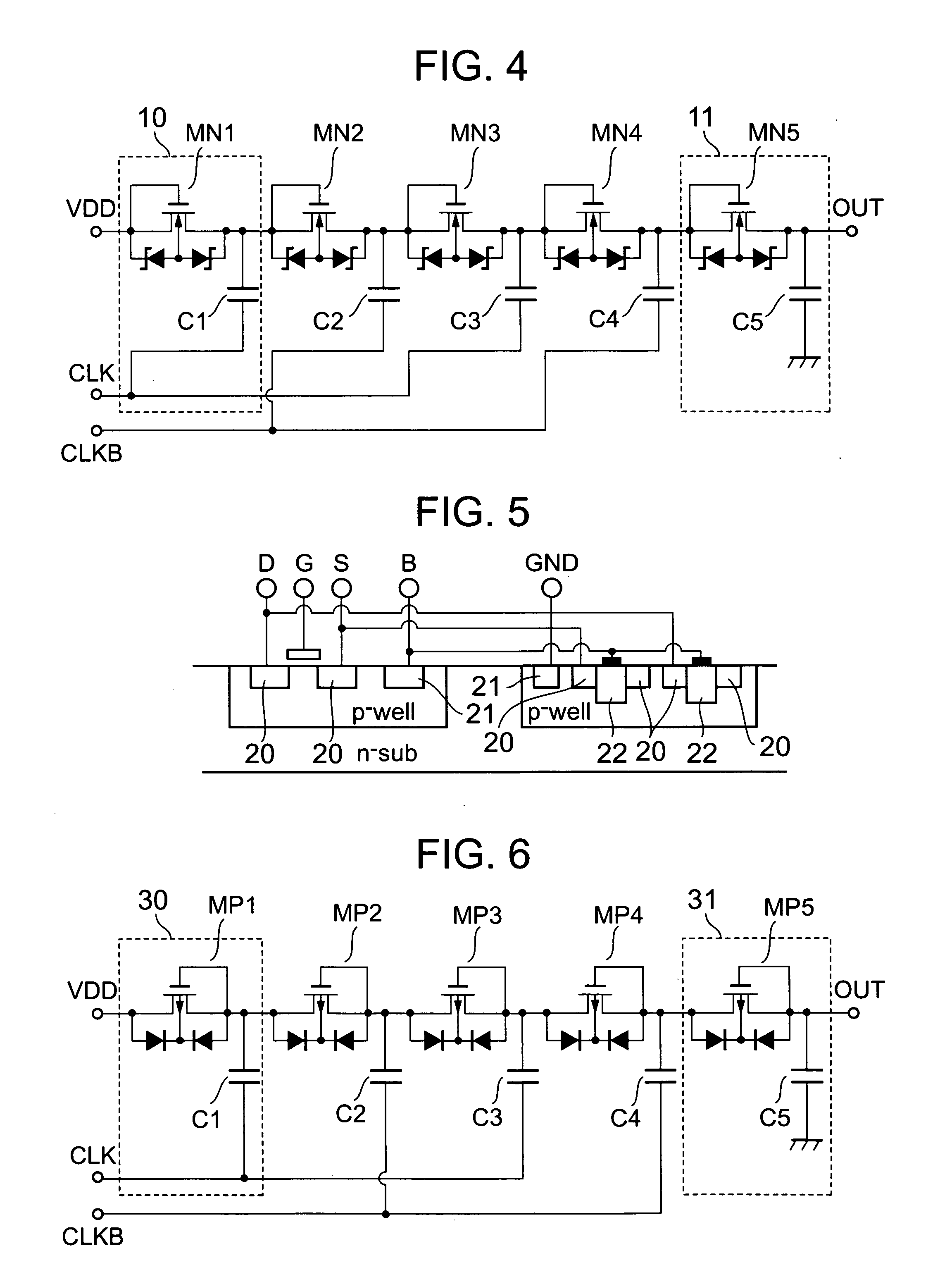
[0055]FIG. 4 shows a third embodiment of a boosting charge pump circuit according to the present invention.

[0056] The difference between the first and third embodiments is that diodes connected to the well, the source, and the drain are Schottky barrier diodes. To be more precise, the parasitic pn-junction diodes are present, so the Schottky barrier diodes are connected in parallel therewith.

[0057]FIG. 5 shows an example of the cross-sectional structure of the n-channel MOS transistor and the Schottky barrier diodes. The cross-sectional structure of the n-channel MOS transistor portion is equal to that shown in FIG. 2. The Schottky barrier diodes are formed through contact between n-wells 22 formed in the p-well connected electrically to the ground GND and a metal (e.g., aluminum). In that case, the metal serves as anodes and the n-wells serve as cathodes. The anodes of the two Schottky barrier diodes are connected in common to the well terminal B of the n-channel MOS transistor. ...


PUM


Abstract

A charge pump circuit is provided which outputs a high voltage by using a boosting circuit with a smaller number of stages. A diode is used to give a back-gate voltage for a MOS transistor composing the charge pump circuit, thereby minimizing a reduction in a boosted voltage due to an increase in the threshold voltage of the MOS transistor. In addition, a second MOS transistor is provided between the back gate of the MOS transistor and the ground (GND) such that in-phase clock signals are inputted to the gate of the second MOS transistor and the capacitor thereof.

Description

BACKGROUND OF THE INVENTION [0001] 1. Field of the Invention [0002] The present invention relates to a charge pump circuit for voltage boosting. [0003] 2. Description of the Related Art [0004] As a conventional charge pump circuit, there has been known a circuit as shown in FIG. 14 (see, e.g., JP 2718375 B (FIG. 11)). [0005] Specifically, n-channel MOS transistors MN1 to MN5 each having the gate and drain thereof connected to each other are connected in series and capacitor elements C1 to C4 are connected individually to the respective connection points between the gates and drains of the MOS transistors MN2 to MN5. To the CLK and CLKB terminals provided at the other end of the capacitor elements, voltages VCLK and VCLKB having phases opposite to each other are inputted, as shown in FIG. 15. [0006] Each of the gate and drain of the n-channel MOS transistor MN1 is connected to a power source VDD and an output OUT of the boosting circuit is extracted from the source of the MOS transis...

Claims


Application Information

Patent Timeline
IPC IPC(8): G11C5/14G11C8/00
CPCG11C5/145H01L27/0222H03K2217/0018H02M3/073H01L27/0727H02M3/07
Inventor SUDOU, MINORU
Owner ABLIC INC
Why Eureka
Try Eureka