Method for simultaneously fabricating ONO-type memory cell, and gate dielectrics for associated high voltage write transistors and gate dielectrics for low voltage logic transistors by using ISSG

a memory cell and gate dielectric technology, applied in the direction of semiconductor devices, basic electric elements, electrical equipment, etc., can solve the problems of contaminating chemicals that can pass through, inter-gates insulator layer (igi), which is typically sandwiched between fg and cg, and still poses numerous problems

Active Publication Date: 2006-01-26
PROMOS TECH INC
View PDF2 Cites 77 Cited by
  • Summary
  • Abstract
  • Description
  • Claims
  • Application Information

AI Technical Summary

Benefits of technology

[0016] Structures and methods may be provided in accordance with the pr...

Problems solved by technology

Such sandwiching of different kinds of dielectric material layers between the gate electrodes, as well as the use of conductive materials to form the gate electrodes can create problems as will be further explained shortly.
Contaminating chemicals can pass through pinhole or other defects in the insulators.
However, the inter-gates insulator layer (IGI) that is typically sandwiched between the FG and the CG still poses numerous problems.
The inter-gates insulator layer (IGI) is particularly prone to problems with excessive leakage current, premature voltage breakdown, and inconsistent mass production results.
Despite improvements in fabrication techniques, the ONO approach still suffers from various problems including the formation of Bird's Beak between the different material layers of the ONO stack.
It is believed that the oxidation-resistant properties of the...

Method used


Image

  • Method for simultaneously fabricating ONO-type memory cell, and gate dielectrics for associated high voltage write transistors and gate dielectrics for low voltage logic transistors by using ISSG
  • Method for simultaneously fabricating ONO-type memory cell, and gate dielectrics for associated high voltage write transistors and gate dielectrics for low voltage logic transistors by using ISSG
  • Method for simultaneously fabricating ONO-type memory cell, and gate dielectrics for associated high voltage write transistors and gate dielectrics for low voltage logic transistors by using ISSG

Examples


Embodiment Construction

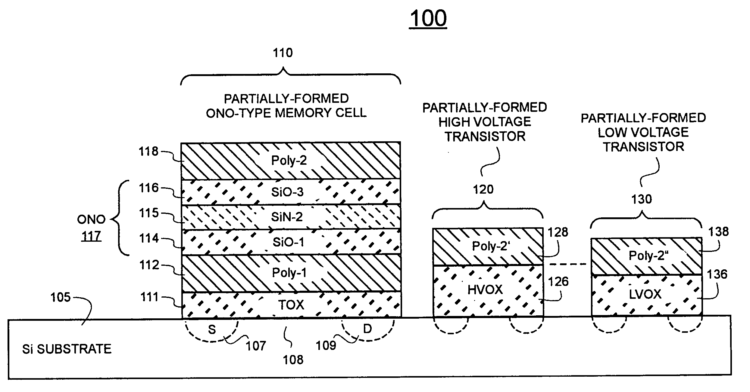
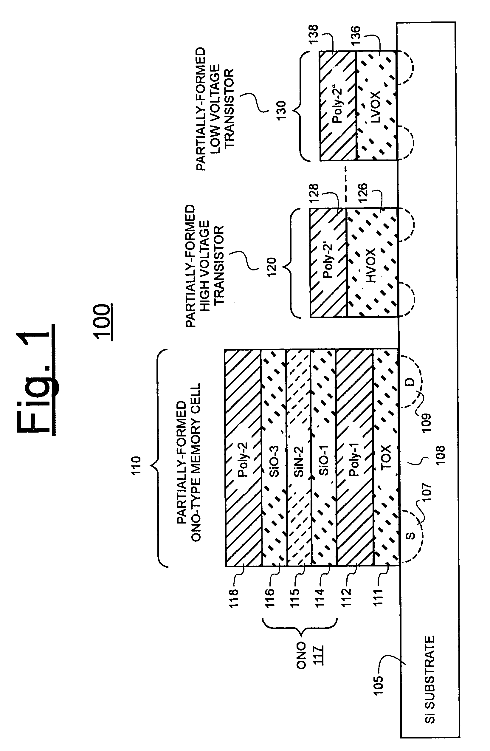
[0031]FIG. 1 is a schematic, side cross sectional diagram showing a partially-completed ONO memory cell stack 110 that has been formed on a monolithic semiconductor substrate 105 and has been positioned adjacent to a partially-completed, high voltage transistor 120 and also adjacent to a partially-completed, low voltage transistor 130. Fabrication of the memory cell and the adjacent low and high voltage transistors is still in progress at this point. More work will be done to finish the integrated circuit. For example, the source and drain regions, 107 and 108, which are not yet present and are thus shown in phantom, will be implanted at a later time and self-aligned to sidewalls other than the ones shown in FIG. 1. Distances and other dimensional aspects shown in the diagram are not to scale. The schematic of FIG. 1 may apply to embodiments of the present invention and also embodiments outside the scope of invention, depending on what process are used to arrive at the schematically...


PUM


Abstract

Conventional fabrication of top oxide in an ONO-type memory cell stack usually produces Bird's Beak. Certain materials in the stack such as silicon nitrides are relatively difficult to oxidize. As a result oxidation does not proceed uniformly along the multi-layered height of the ONO-type stack. The present disclosure shows how radical-based fabrication of top-oxide of an ONO stack (i.e. by ISSG method) can help to reduce formation of Bird's Beak. More specifically, it is indicated that short-lived oxidizing agents (e.g., atomic oxygen) are able to better oxidize difficult to oxidize materials such as silicon nitride and the it is indicated that the short-lived oxidizing agents alternatively or additionally do not diffuse deeply through already oxidized layers of the ONO stack such as the lower silicon oxide layer. As a result, a more uniform top oxide dielectric can be fabricated with more uniform breakdown voltages along its height. Additionally, adjacent low and high voltage transistors may benefit from simultaneous formation of their gate dielectrics with use of the radical-based oxidizing method.

Description

1. FIELD OF DISCLOSURE [0001] The present invention relates generally to fabrication of monolithically integrated semiconductor devices. [0002] The invention relates more specifically to the formation in a monolithic device of gate insulation for a charge-retaining structure used in non-volatile reprogrammable memory such as the type generically known as an ONO stack and to the simultaneous formation of gate dielectric for associated high voltage transistors and to the simultaneous formation of gate dielectric for low voltage transistors. 2a. CROSS REFERENCE TO CO-OWNED APPLICATIONS [0003] The following copending U.S. patent applications are owned by the owner of the present application, and their disclosures are incorporated herein by reference: [0004] (A) Ser. No. 10 / 442,759 [Attorney Docket No. M-12978] filed May 20, 2003 by Zhong Dong et al. and which is originally entitled, Methods for Improving Quality of High Temperature Oxide (HTO) Formed from Halogen-Containing Precursor an...

Claims


Application Information

Patent Timeline
IPC IPC(8): H01L21/8242H01L21/336
CPCH01L21/28273H01L27/105H01L29/42324H01L27/11546H01L27/11526H01L29/40114H10B41/40H10B41/49
Inventor DONG, ZHONGJANG, CHUCKCHEN, CHING-HWAHSIAO, CHIA-SHUN
Owner PROMOS TECH INC
Why Eureka
Try Eureka