Heterogeneous organic laminate stack ups for high frequency applications

a stacking and organic technology, applied in the direction of printed circuit manufacturing, printed circuit non-printed electric components association, printed circuit aspects, etc., can solve the problems of system performance suffer, the overall size of the printed circuit board assembly, and many challenges, so as to reduce the interconnection length, improve reliability, and reduce the effect of system siz

Active Publication Date: 2006-01-26
KYOCERA AVX COMPONENTS CORP
View PDF98 Cites 36 Cited by
  • Summary
  • Abstract
  • Description
  • Claims
  • Application Information

AI Technical Summary

Benefits of technology

[0008] Embodiments of the present invention disclose materials stack up, sequences, and process fabrication techniques for embedding active and passive discrete devices within one or more organic layers and / or cavities. The materials stack up coupled with novel process features allows for the generation of new topologies that result in reduced layer counts and increased component density, thereby resulting in very high component densities.

Problems solved by technology

The above-described process, although widely used to reduce the overall size of the printed circuit board assembly, still has many challenges.
These challenges include microminiaturization, reliability, and performance.
In any case, system performance suffers.

Method used


Image

  • Heterogeneous organic laminate stack ups for high frequency applications
  • Heterogeneous organic laminate stack ups for high frequency applications
  • Heterogeneous organic laminate stack ups for high frequency applications

Examples


Embodiment Construction

[0029] The present invention now will be described more fully hereinafter with reference to the accompanying drawings, in which preferred embodiments of the invention are shown. This invention may, however, be embodied in many different forms and should not be construed as limited to the embodiments set forth herein; rather, these embodiments are provided so that this disclosure will be thorough and complete, and will fully convey the scope of the invention to those skilled in the art. Like numbers refer to like elements throughout.

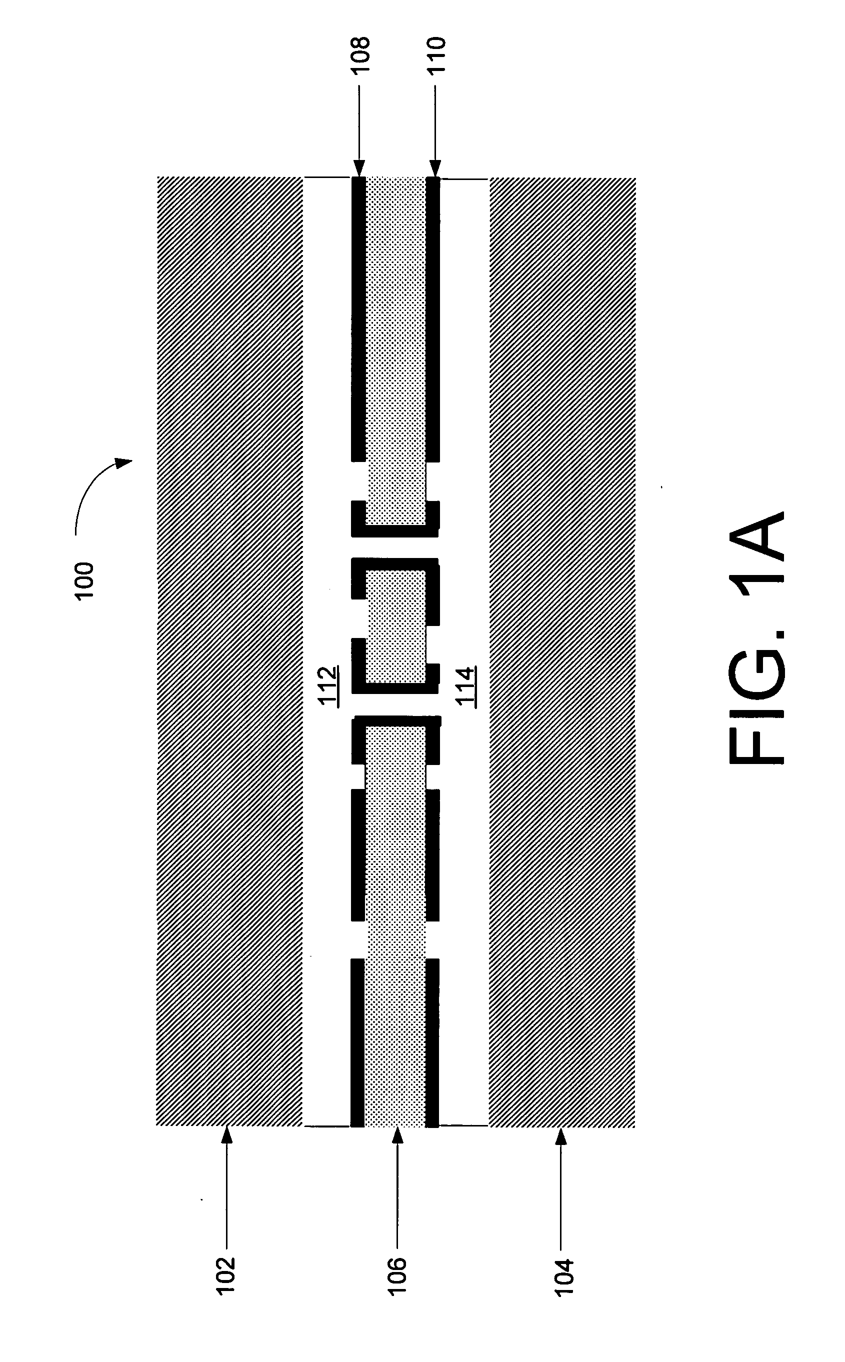
[0030] According to an embodiment of the invention, an exemplary heterogeneous organic materials structure will now be described with reference to FIG. 1A. The outer layers 102, 104 of the stack up 100 may include thermoplastics such as Rogers 4350 or Rogers 4003, liquid crystalline polymer (LCP), or other organic material such as hydrocarbon, Teflon, epoxy, or polyimide. The Rogers material is available from the Rogers Corporation headquartered in Roger...


PUM


Abstract

Organic laminate stack ups are disclosed for a variety of applications, including high frequency RF applications. One or more inner core layers may be disposed between outer layers along with bondply or prepreg layers as needed. Discrete devices, including surface mount components and flip chips, may be embedded within the organic laminate stack up structures. The embedding of the discrete devices, which may be active or passive devices, may be in the form of a layer of bondply or prepreg encapsulating the discrete devices. In addition or in the alternative, cavities may be formed in at least the outer layers for housing discrete devices, which include surface mount components, flip chips, and wire bonded integrated circuits. A variety of caps may be utilized to seal the cavities. Further, shielding may be provided for the organic laminate stack up structure, including through a wall of vias or a plated trench cut along at least one side of the stack up structure. Each stack up structure may be packaged in a variety of ways, including as a surface mount component, ball grid array, or land grid array.

Description

RELATED APPLICATIONS [0001] The present application claims priority to U.S. Provisional Patent Application Ser. No. 60 / 586,200 filed Jul. 8, 2004, which is hereby incorporated by reference as if set forth fully herein.BACKGROUND OF THE INVENTION [0002] 1. Field of the Invention [0003] Aspects of the present invention relate generally to integrated devices and more particularly to organic laminate stack ups. [0004] 2. Description of the Related Art [0005] Today typical printed circuit board assembly processes can be categorized into two modes of assembly: a) through hole assembly and b) surface mount assembly (SMA). While both are used widely, SMA is the generally preferred assembly method when an objective is to reduce size and increase performance. Using SMA processes, one can readily assemble both active and passive components, which may be generally referred to as surface mount devices (SMD). Surface mount active and passive components typically have been placed on the outermost ...

Claims


Application Information

Patent Timeline
Patent Type & Authority Applications(United States)
IPC IPC(8): H01L23/12
CPCH01L21/4857H01L2924/01019H01L23/13H01L23/49827H01L23/49833H01L23/5383H01L23/5389H01L2224/16225H01L2224/48091H01L2224/73253H01L2924/01078H01L2924/01079H01L2924/09701H01L2924/15153H01L2924/15165H01L2924/1517H01L2924/15311H01L2924/16152H01L2924/16195H01L2924/19041H01L2924/19105H01L2924/3025H05K1/183H05K1/186H05K2201/09509H05K2201/09536H05K2203/061H01L23/055H01L2224/48227H01L24/48H01L2924/00014H01L2224/73265H01L2924/00011H01L2924/14H01L2924/181H01L2924/00012H01L2924/00H01L2224/0401H01L2224/45099H01L2224/45015H01L2924/207
Inventor WHITE, GEORGE E.DALMIA, SIDHARTHSUNDARAM, VENKATESHSWAMINATHAN, MADHAVAN
Owner KYOCERA AVX COMPONENTS CORP
Why Eureka
Try Eureka