Processing multilayer semiconductors with multiple heat sources

a multi-layer semiconductor and heat source technology, applied in the field of semiconductor processing, can solve the problems of preventing dopant penetration, requiring low thermal budget activation annealing, and increasing the difficulty of maintaining balance, so as to achieve rapid thermal annealing and rapid thermal annealing

Active Publication Date: 2006-01-26
APPLIED MATERIALS INC
View PDF101 Cites 142 Cited by
  • Summary
  • Abstract
  • Description
  • Claims
  • Application Information

AI Technical Summary

Benefits of technology

[0012] The present invention generally provides a chamber for rapid thermal annealing comprising a plurality of lamps affixed to a lid of the chamber that provide at least one wavelength of light, a laser source extending into the chamber, a substrate support extending through a base of the chamber, an edge ring affixed to the substrate support, and a gas distribution assembly in communication with the lid and the base of the chamber. The ...

Problems solved by technology

Activating the polysilicon gate electrode without causing dopant diffusion is a major challenge for front end of line (FEOL) processing.
The balance becomes more difficult to maintain as device makers try to overcome poly-depletion.
Conventional thermal processes are not capable of annealing such small substrate features without provoking dopant diffusion.
In addition, preventing dopant penetration and use of thermally sensitive high-k materials requires low thermal budget activation anneal.
Laser annealing technology ...

Method used


Image

  • Processing multilayer semiconductors with multiple heat sources
  • Processing multilayer semiconductors with multiple heat sources
  • Processing multilayer semiconductors with multiple heat sources

Examples


Embodiment Construction

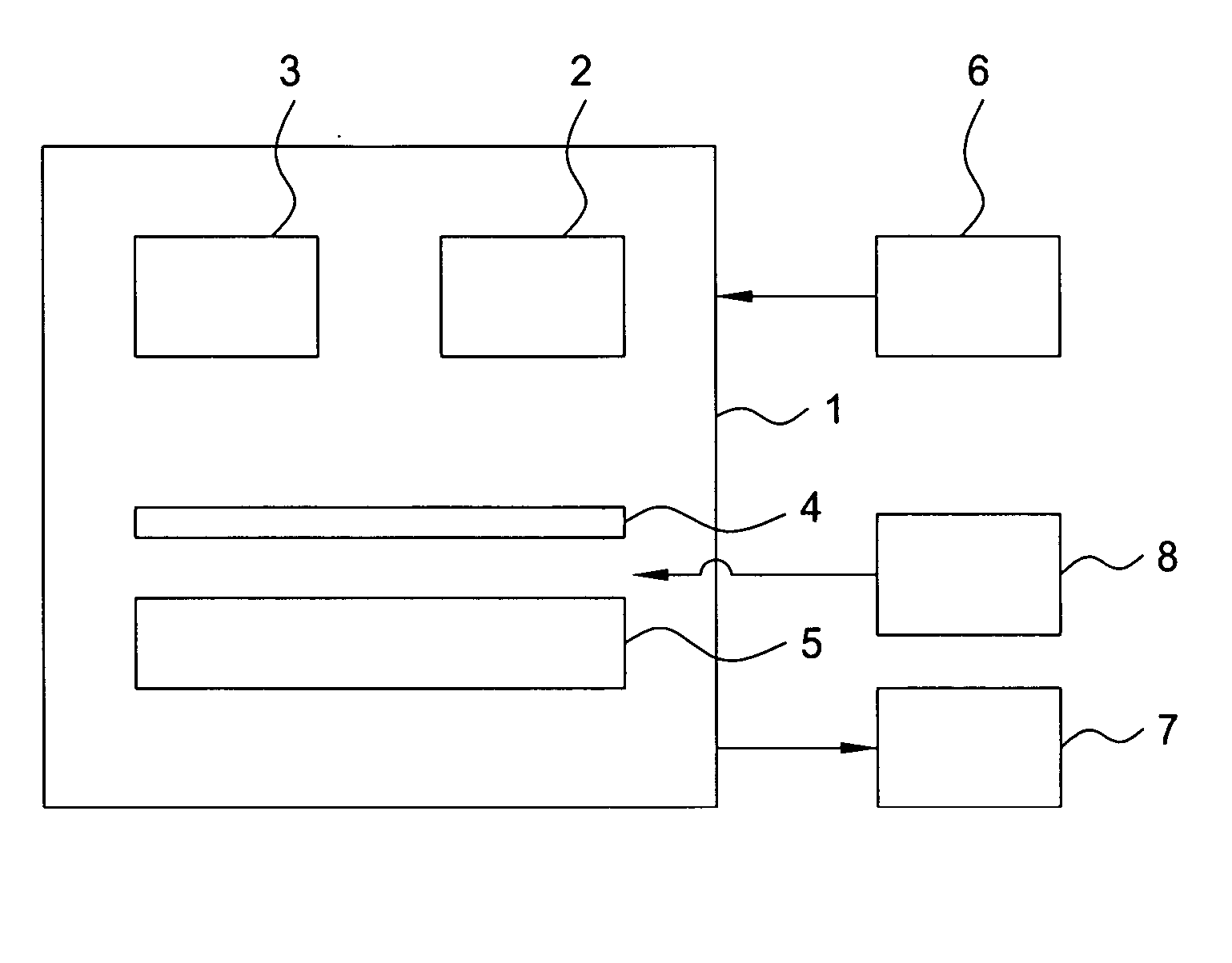
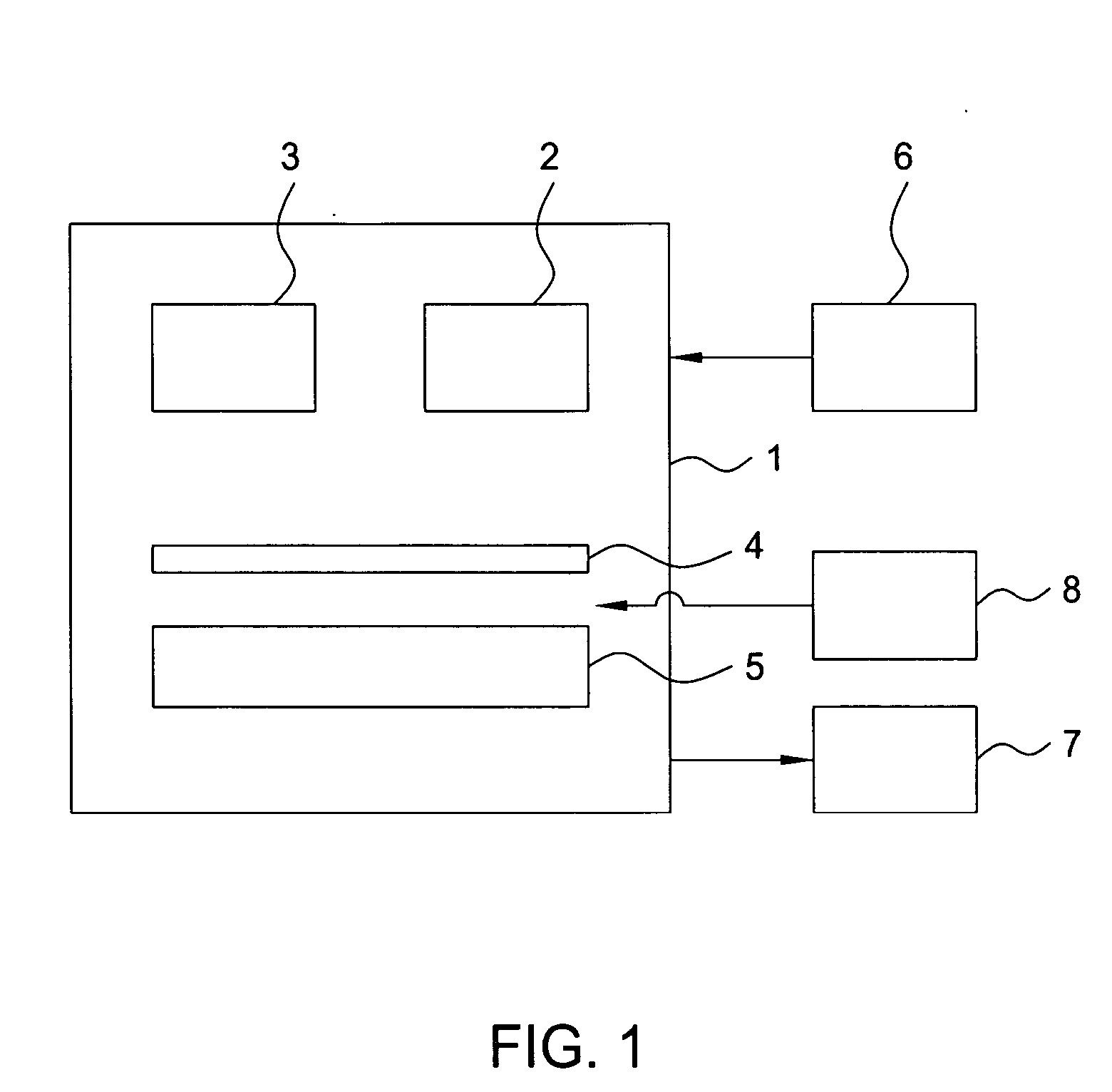
[0020] A combination of approaches is used to create an RTP chamber with a controllable temperature profile that compensates for heat transfer non-uniformity in the chamber. Furthermore, a non-uniform temperature gradient can provide downstream or upstream processing correction for electrical, thickness, chemical, or crystalline imperfections in substrates. For example, a non-uniform temperature gradient can be tailored to compensate for front-side emissivity variation for individual wafers and provide improved silicon containing film deposition.

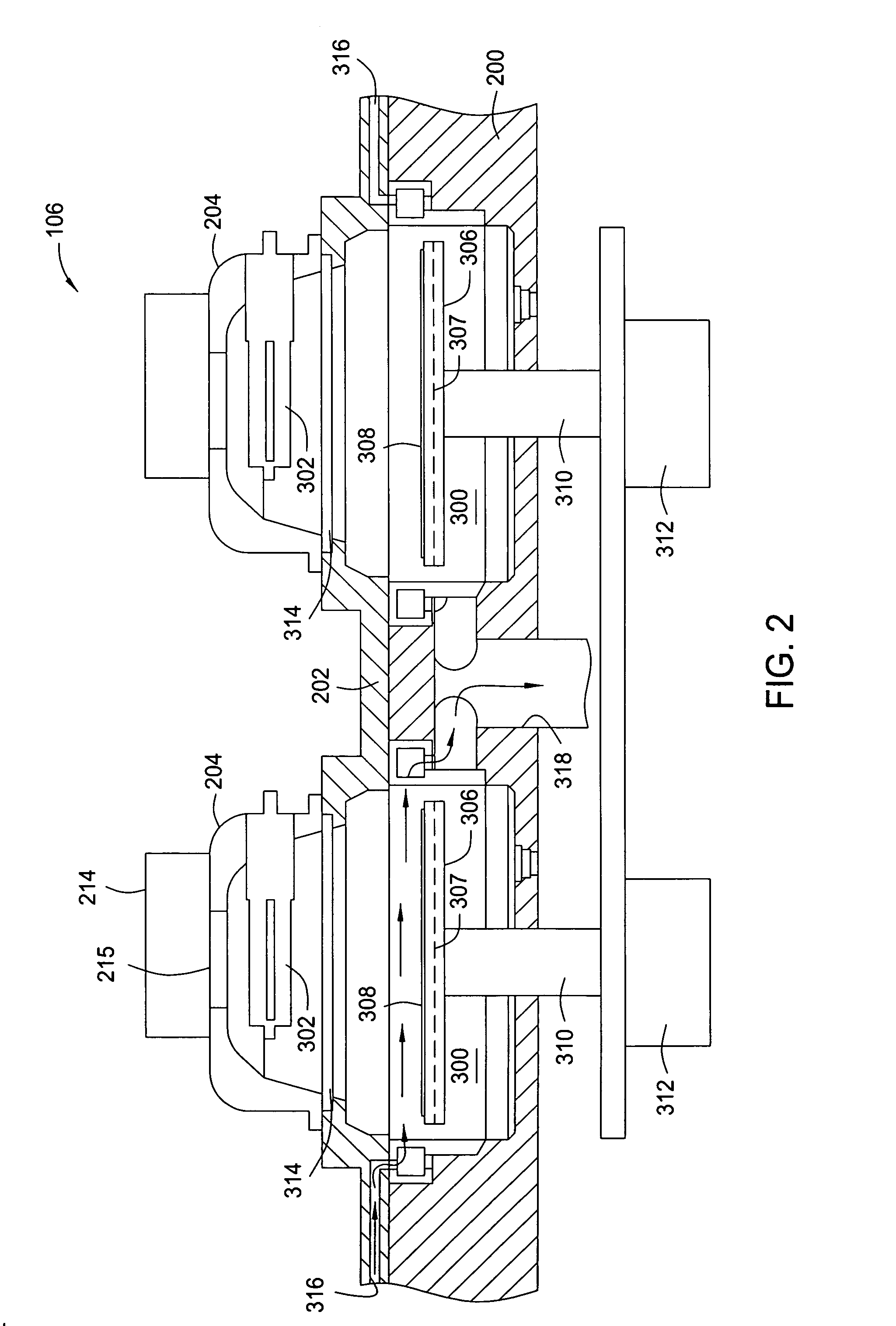
[0021] A substrate can be measured for certain characteristics such as emissivity or stack thickness prior to processing in the RTP chamber. The emissivity of the system can be either directly measured or estimated based on the stack thickness. The direct measurement of the emissivity may increase the accuracy of the compensation system. There are several options for measuring the emissivity. An internal pyrometer may be used and located wi...


PUM


Abstract

A method and apparatus for rapid thermal annealing comprising a plurality of lamps affixed to a lid of the chamber that provide at least one wavelength of light, a laser source extending into the chamber, a substrate support positioned within a base of the chamber, an edge ring affixed to the substrate support, and a gas distribution assembly in communication with the lid and the base of the chamber. A method and apparatus for rapid thermal annealing comprising a plurality of lamps comprising regional control of the lamps and a cooling gas distribution system affixed to a lid of the chamber, a heated substrate support with magnetic levitation extending through a base of the chamber, an edge ring affixed to the substrate support, and a gas distribution assembly in communication with the lid and the base of the chamber.

Description

CROSS-REFERENCE TO RELATED APPLICATIONS [0001] This application is a continuation-in-part of co-pending U.S. patent application Ser. No. 10 / 950,145, filed Sep. 24, 2004, which claims benefit of U.S. provisional patent application Ser. No. 60 / 515,037, filed Oct. 27, 2003. Each of the aforementioned related patent applications is herein incorporated by reference.BACKGROUND OF THE INVENTION [0002] 1. Field of the Invention [0003] The present invention relates generally to the field of semiconductor processing and, more specifically, to thermal annealing during semiconductor device fabrication. [0004] 2. Description of the Related Art [0005] Rapid thermal processing (RTP) is a process for annealing substrates during semiconductor fabrication. During this process, thermal radiation is used to rapidly heat a substrate in a controlled environment to a maximum temperature of over nine hundred degrees above room temperature. This maximum temperature is maintained for less than one second to ...

Claims


Application Information

Patent Timeline
IPC IPC(8): A21B2/00H01L21/00
CPCH01L21/67103
Inventor RAMAMURTHY, SUNDARHEGEDUS, ANDREAS G.THAKUR, RANDHIR
Owner APPLIED MATERIALS INC
Why Eureka
Try Eureka