
Variable gain amplifier circuit and radio machine

a gain amplifier and amplifier circuit technology, applied in the direction of gain control, analog signal digital control, manual operation gain control, etc., can solve the problem of constant current consumption and achieve the effect of reducing current and free of deterioration of distortion characteristics

Inactive Publication Date: 2006-02-02
PANASONIC CORP
View PDF3 Cites 16 Cited by
  • Summary
  • Abstract
  • Description
  • Claims
  • Application Information

AI Technical Summary

Benefits of technology

[0019] With the arrangement above, the current decreases when the voltage gain is lowered and it is possible to achieve the effect of enlarging the dynamic range of gain control in addition to the effect of substantially obviating a deterioration in distortion characteristics represented by the suppression ratio.
[0055] With the arrangement above, it is possible to decrease the current when the voltage gain is lowered in the radio circuits and to realize a radio communication apparatus substantially free of a deterioration in distortion characteristics.

Problems solved by technology

Therefore, the problem is that because the conventional variable gain amplifier circuit as the first example always consumes a relatively large current irrespective of the voltage gain, the current consumed thereby never decreases even though the voltage gain is lowered.

Method used


Image

  • Variable gain amplifier circuit and radio machine
  • Variable gain amplifier circuit and radio machine
  • Variable gain amplifier circuit and radio machine

Examples


first embodiment

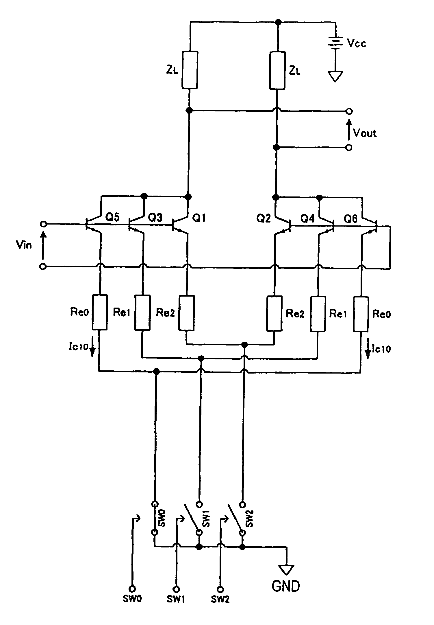
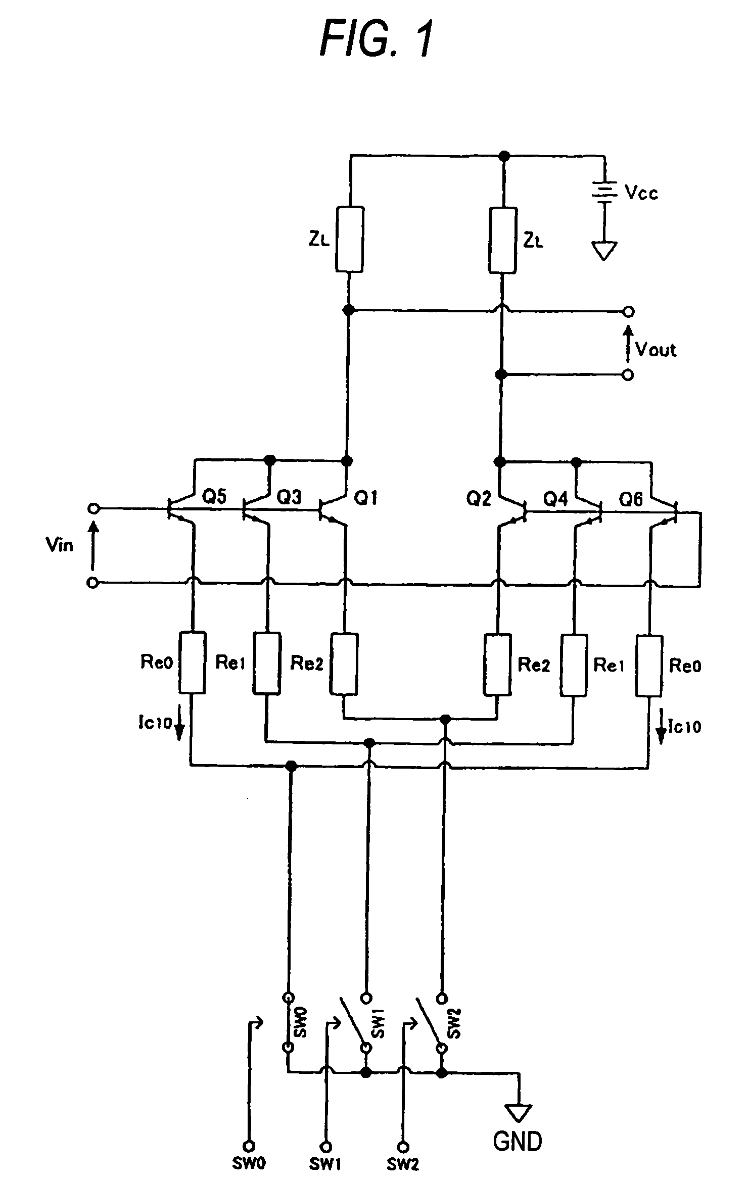
[0094]FIG. 1 is a circuit diagram showing a variable gain amplifier circuit according to a first embodiment of the invention.

[0095] The variable gain amplifier circuit according to the first embodiment of the invention is formed such that the bases of bipolar transistors Q1, Q3 and Q5 and the bases of bipolar transistors Q2, Q4 and Q6 are connected in common with each other, these bipolar transistors forming a plurality of common-emitter amplifier circuits; a switch SW2 is connected to the emitter sides of the bipolar transistors Q1 and Q2; a switch SW1 to the emitter sides of bipolar transistors Q3 and Q4; and a switch SW0 to the emitter sides of the bipolar transistors Q5 and Q6. Thus, the desired common-emitter amplifier circuit can be selected by each of the switches SW2, SW1 and SW0.

[0096] With the arrangement of FIG. 1, when any emitter side of a bipolar transistor pair is held at ground potential gnd by switching on / off the switches SW2, SW1 and SW0 by means of a control si...

second embodiment

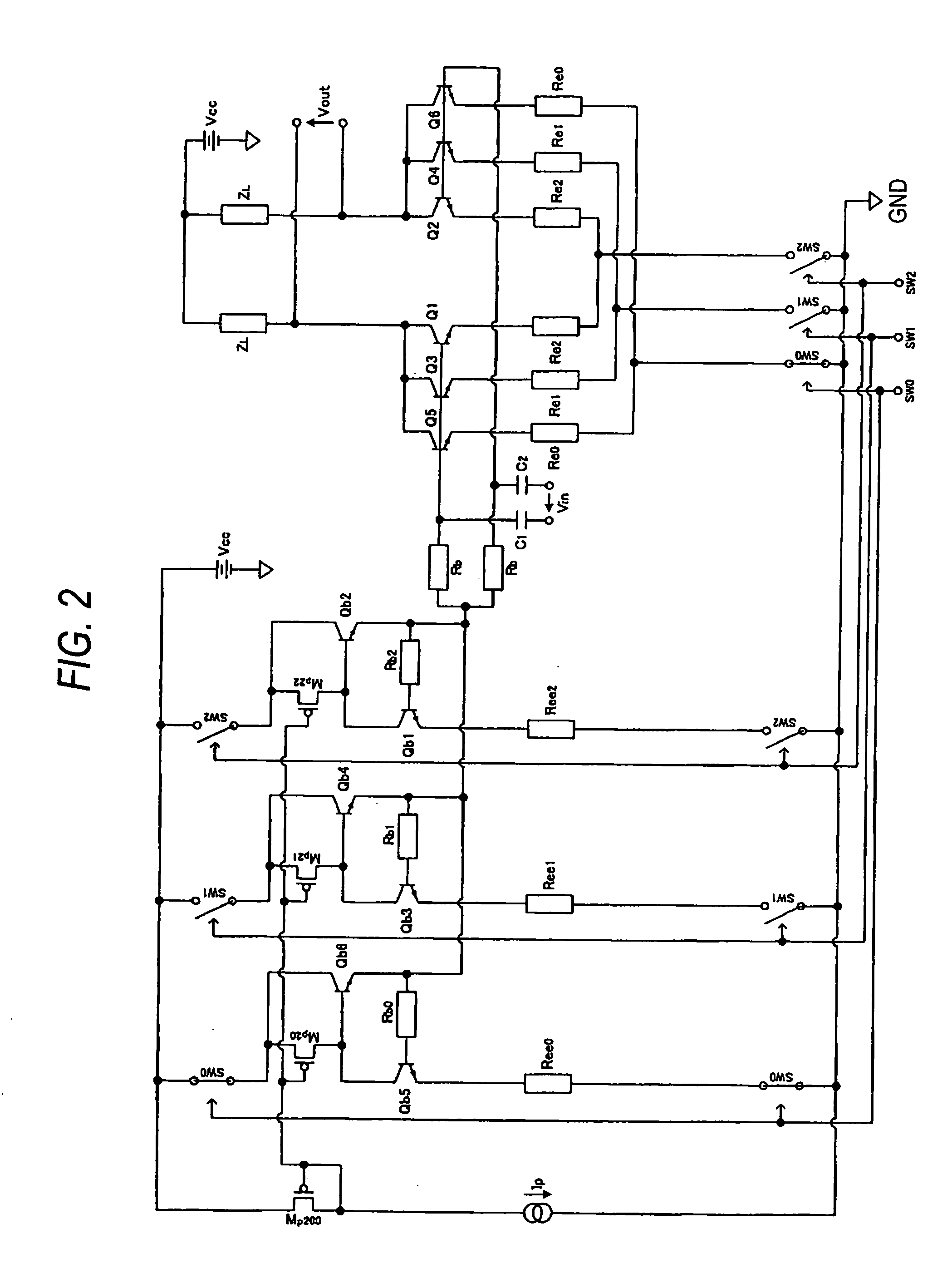
[0108]FIG. 5 is a circuit diagram showing a variable gain amplifier circuit configuration according to a second embodiment of the invention.

[0109] The variable gain amplifier circuit according to the second embodiment of the invention is such that the differential type circuit in the differential form shown in FIG. 1 according to the first embodiment of the invention is changed to a single-ended type one. This variable gain amplifier circuit is formed such that the bases of bipolar transistors Q1, Q3 and Q5 forming a plurality of common-emitter amplifier circuits are connected in common with each other and that switches SW2, SW1 and SW0 are connected to the respective emitter sides thereof.

[0110] The circuit operation is the same as what is described in the first embodiment of the invention. When the emitter side of any bipolar transistor is held at the ground potential gnd in the configuration of FIG. 5 by switching the switches SW2, SW1 and SW0, the bipolar transistor operates a...

third embodiment

[0112]FIG. 6 is a circuit diagram showing a variable gain amplifier circuit configuration according to a third embodiment of the invention. The third embodiment of the invention refers to a partially modified example of the first embodiment of the invention above.

[0113] The difference in configuration between the third embodiment of the invention and the first embodiment thereof is that emitter degeneration resistors Rec0, Rec1 and Rec2 in phase are added to the respective bipolar transistor pairs; the rest is configured as in the first embodiment thereof. The resistance value ratio of each of the emitter degeneration resistors Rec0, Rec1 and Rec2 in phase is set inversely proportional to the emitter area ratio like the emitter degeneration resistors Re0, Re1 and Re2 so as to satisfy the relation of an equation 6c below.

Rec0 / 4=Rec1 / 2=Rec2  (6c)

[0114] The collector current ratio can thus be kept constant. As the voltage gain of the in-phase signal is made reducible by adding the e...


PUM


Abstract

A variable gain amplifier circuit is provided so that an electric current decreases when a voltage gain is lowered and that the amplifier circuit is substantially free of a deterioration in distortion characteristics. The bases of bipolar transistors Q1, Q3 and Q5 and the bases of bipolar transistors Q2, Q4 and Q6 are connected in common with each other, these bipolar transistors forming a plurality of common-emitter amplifier circuits, and switches SW2, SW1 and SW0 are connected to the respective sides of the bipolar transistors. The emitter sides are held at a ground potential gnd by switching the switches SW2, SW1 and SW0 so that the voltage gain is controlled by selecting the common-emitter amplifier circuits different in voltage gain. A collector current I0 and an emitter degeneration resistance Re between the common-emitter amplifier circuits are so arranged as to have different values. The ratio of the collector current I0 is set inversely proportional to the ratio of the emitter degeneration resistance Re, whereby the collector current I0 decreases when the voltage gain is lowered and a deterioration in distortion characteristics is substantially obviated.

Description

TECHNICAL FIELD [0001] The present invention relates to a variable gain amplifier circuit and a radio communication apparatus fitted with the same. BACKGROUND ART [0002] Conventional variable gain amplifier circuits are shown in FIGS. 32-34 by way of example. The conventional variable gain amplifier circuit shown in FIG. 32 as a first example is formed with a pair of common-emitter amplifier circuits having bipolar transistors Q1 and Q2, and differential pairs of bipolar transistors Q3 and Q4 and bipolar transistors Q5 and Q6. With this arrangement, an input signal Vin is fed into the bases of the bipolar transistors Q1 and Q2 and the output current of the common-emitter amplifier circuit branches out in accordance with a gain control voltage Vgc fed into the bases of the bipolar transistors Q3-Q6 forming the differential pair. The voltage gain Av2 of the variable gain amplifier circuit is expressed by an equation 1a below and controlled by the gain control voltage Vgc under the ass...

Claims


Application Information

Patent Timeline
IPC IPC(8): H03F1/14H03F3/45H03G3/10H03G1/00H03G3/00H03G3/02
CPCH03F2203/45362H03F2203/45504H03F2203/45616H03G3/001H03G1/0023H03G1/0029H03G1/0088H03F2203/7203
Inventor UDAGAWA, MASAHARU
Owner PANASONIC CORP
Learn More