Power supply antenna and power supply method

a technology of power supply antenna and power supply method, which is applied in the direction of individual energised antenna array, plasma technique, coating, etc., can solve the problem that the uniformity of film thickness on the surface of the wafer cannot be guaranteed by film deposition, and achieves uniform film thickness, high quality, and minimal power loss

Inactive Publication Date: 2006-02-09
MITSUBISHI HEAVY IND LTD
View PDF14 Cites 7 Cited by
  • Summary
  • Abstract
  • Description
  • Claims
  • Application Information

AI Technical Summary

Benefits of technology

[0013] According to this aspect, disturbances in the electric field and the magnetic field due to the Ez can be dispersed most satisfactorily in the circumferential direction. Thus, the effects of the invention in the aspect 1) can be obtained most markedly. That is, an electromagnetic wave most uniform in the circumferential direction (θ direction) can be generated. 5) A power supply apparatus including a power supply antenna comprising a plurality of coils disposed concentrically, the plurality of coils being prepared by bending a plurality of conductors each into the form of an arc, and matching means having capacitors connected in parallel to the respective coils of the power supply antenna, and wherein the matching means has a first tubular capacitor and a second tubular capacitor each having electrodes at axially opposite ends thereof, and also has a first electrode, a second electrode and a third electrode disposed parallel to the power supply antenna, with electrical insulation being established with respect to each other, one of the electrodes of the first capacitor being connected to the first electrode, one of the electrodes of the second capacitor being connected to the second electrode, and the other electrodes of the first and second capacitors being connected to the third electrode.
[0014] According to this aspect, a uniform electromagnetic wave can be generated by the power supply apparatus ensuring impedance matching to the power supply antenna. Thus, a uniform plasma can be effectively generated by the electromagnetic wave with a uniform maximum intensity. 6) In the power supply apparatus described in the aspect 5), the first electrode and the third electrode of the matching means may be disposed at opposite ends thereof, the second electrode comprising a flat plate portion having through-holes and a concave portion protruding from the flat plate portion toward the first electrode may be disposed between the first electrode and the third electrode, the first capacitor may pass through the through-hole and may have one of the electrodes thereof connected to the first electrode, the second capacitor may fit into the concave portion and may have one of the electrodes thereof connected to the second electrode, and at least one of power supply portions of each of the coils constituting the power supply antenna may pass through at least the first electrode and establish an electrically connected relationship with the second electrode.
[0015] According to this aspect, the degree of freedom of selecting the positions of connection between the plurality of power supply portions in different phases and the first and second electrodes is maximized. Thus, the lengths of the power supply portions are rendered as short as possible to minimize power losses at the sites of connection. In this state, electrical connection between the power supply antenna and the first and second electrodes can be established. 7) In the power supply apparatus described in the aspect 5) or 6), the power supply antenna may be the same as the power supply antenna described in the aspect 1). Thus, the same effects as those of the invention described in the aspect 1) can be obtained. 8) In the power supply apparatus described in the aspect 5) or 6), the power supply antenna may be the power supply antenna described in the aspect 2). Thus, the same effects as those of the invention described in the aspect 2) can be obtained. 9) In the power supply apparatus described in the aspect 5) or 6), the power supply antenna may be the power supply antenna described in the aspect 3). Thus, the same effects as those of the invention described in the aspect 3) can be obtained. 10) In the power supply apparatus described in the aspect 5) or 6), the power supply antenna may be the power supply antenna described in the aspect 4). Thus, the same effects as those of the invention described in the aspect 4) can be obtained. 11) A semiconductor manufacturing apparatus comprising a vessel having an electromagnetic wave transparent window, a power supply antenna provided outside the vessel and opposed to the electromagnetic wave transparent window, and a power source for applying a high frequency voltage to the power supply antenna, and being adapted to apply the high frequency voltage from the power source to the power supply antenna to generate an electromagnetic wave, and pass the electromagnetic wave through the electromagnetic wave transparent window into the vessel to generate a plasma, thereby treating the surface of a substrate in the vessel, the semiconductor manufacturing apparatus having the power supply antenna or the power supply apparatus described in any one of the aspects 1) to 10).
[0016] According to this aspect, a uniform plasma distribution can be formed in the vessel. Thus, a high quality semiconductor product with a uniform film thickness can be obtained. 12) A power supply method for the power supply antenna, the power supply apparatus, or the semiconductor manufacturing apparatus described in any one of the aspects 1) to 11), wherein the frequency of a high frequency voltage applied to the coil on the outermost periphery of the power supply antenna is made relatively lower than the frequency of a high frequency voltage applied to the other coil, whereby heating of a plasma directly below the coil on the outermost periphery is promoted.
[0017] According to this aspect, the amount of electromagnetic energy absorption by the plasma directly below the coil on the outermost periphery can be increased. Thus, a high temperature, high density plasma can be generated even near the wall surface of the vessel. 13) The power supply apparatus described in any one of the aspects 5) to 10), which may include a plurality of types of power sources for supplying high frequency voltages of different frequencies, and wherein the high frequency power source for an output voltage of the lowest frequency may be connected to the coil on the outermost periphery, and the high frequency power source for an output voltage of a relatively high frequency may be connected to the other coil.
[0018] According to this aspect, the amount of electromagnetic energy absorption by a plasma directly below the coil on the outermost periphery can be increased. Thus, a high temperature, high density plasma can be generated even near the wall surface of the vessel. 14) The semiconductor manufacturing apparatus described in the aspect 11), which may include a plurality of types of power sources for supplying high frequency voltages of different frequencies, and wherein the high frequency power source for an output voltage of the lowest frequency may be connected to the coil on the outermost periphery, and the high frequency power source for an output voltage of a relatively high frequency may be connected to the other coil.

Problems solved by technology

Hence, film deposition cannot ensure the uniformity of the film thickness throughout the surface of the wafer 04.

Method used


Image

  • Power supply antenna and power supply method
  • Power supply antenna and power supply method
  • Power supply antenna and power supply method

Examples


first embodiment

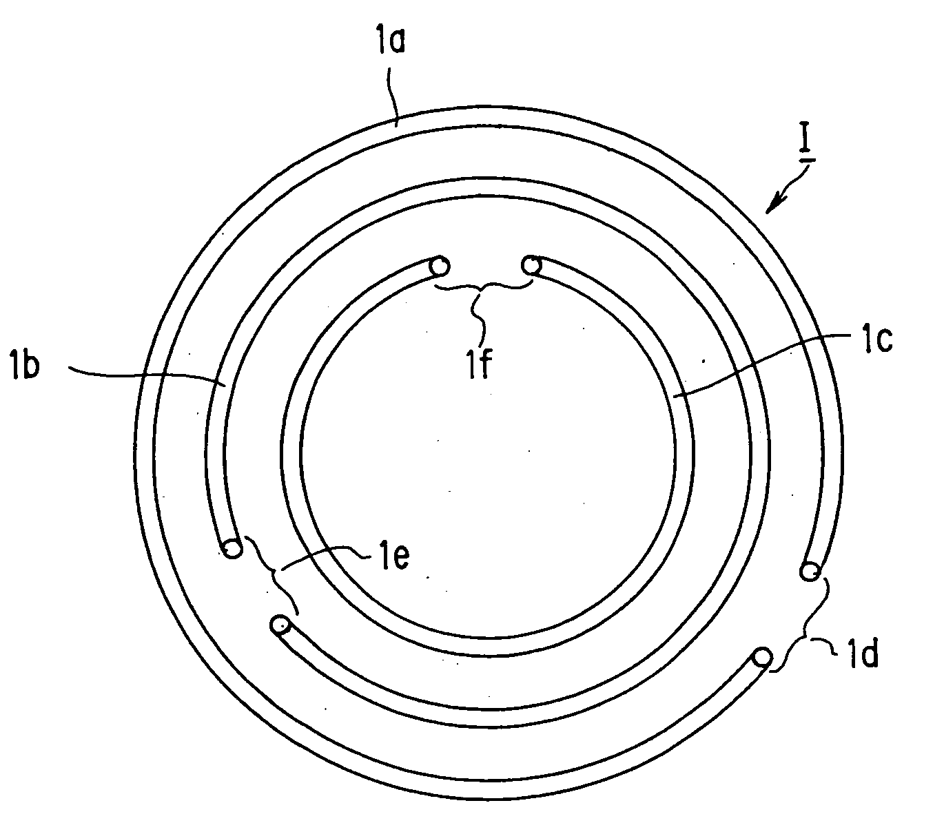
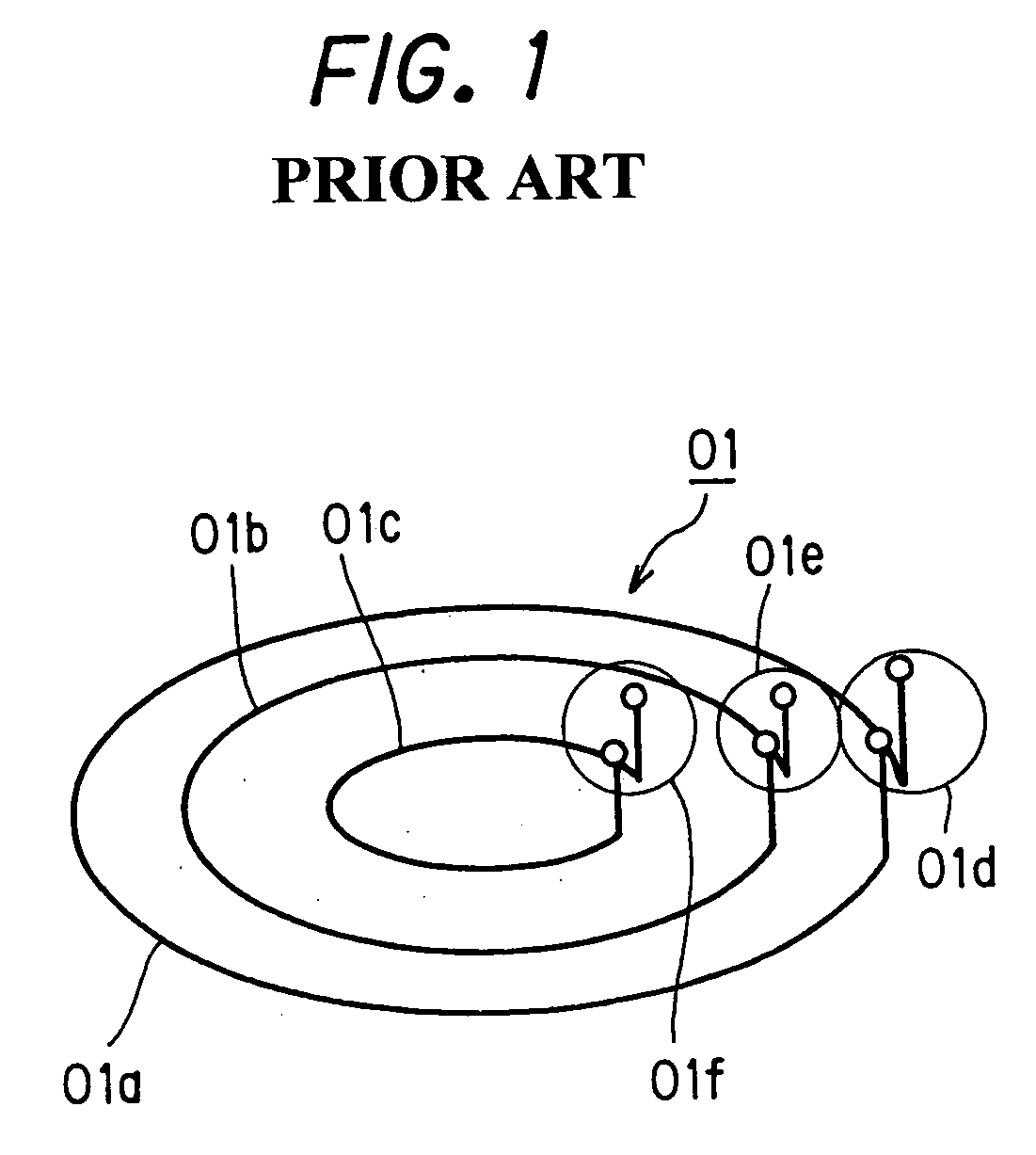
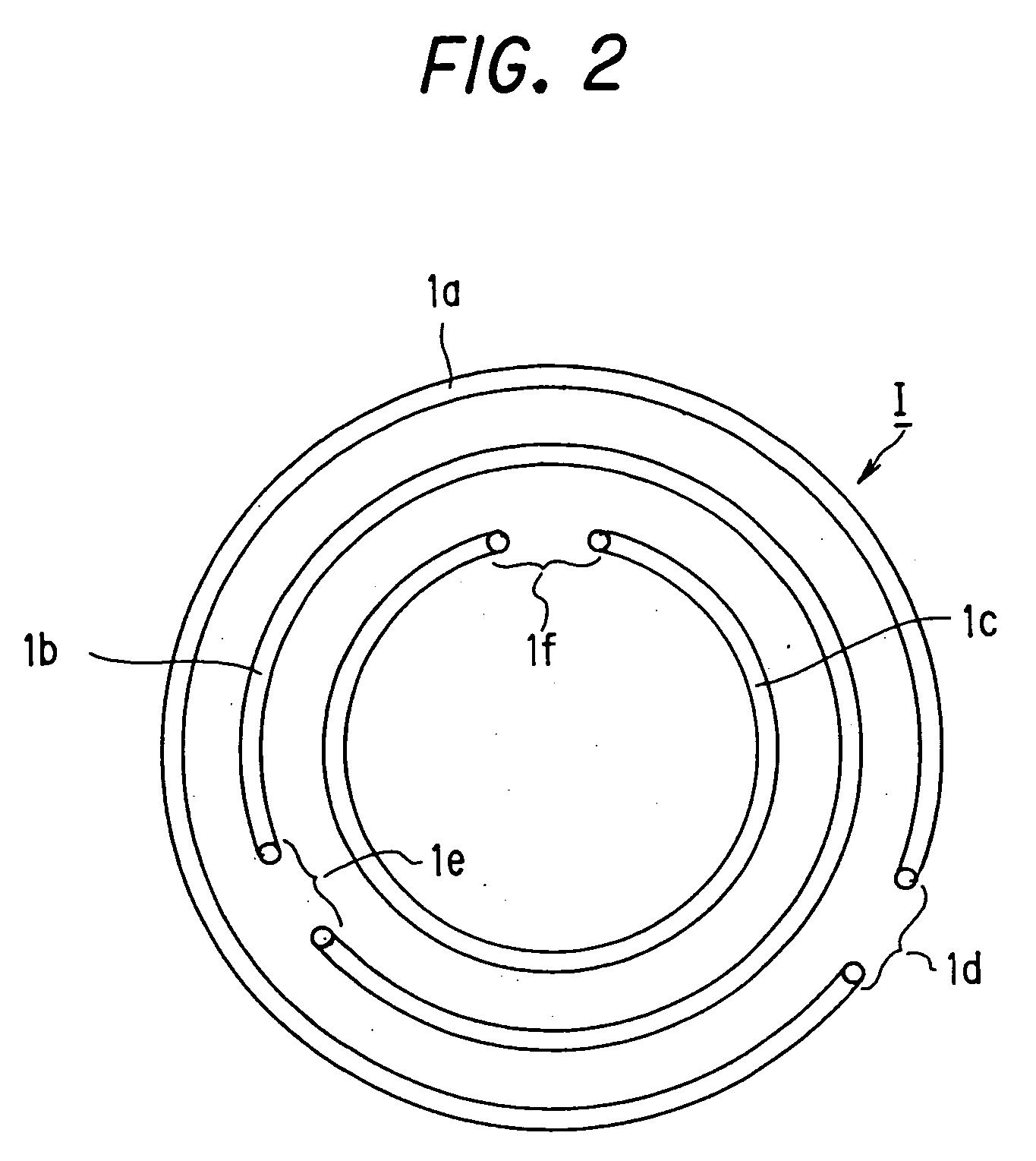
[0035] In the power supply antenna 01 comprising a concentric arrangement of the plural coils, 01a, 01b and 01c prepared by bending the plurality of conductors each into the form of an arc, the embodiment shown in FIG. 2 proposes that the disturbances in the electric field and the magnetic field at the power supply portions 01d, 01e and 01f be dispersed in the circumferential direction to minimize the influence of the Z-direction component Ez. FIG. 2 is a plan view showing a power supply antenna according to the present invention. As shown in the drawing, a power supply antenna I comprises a concentric arrangement of a plurality of coils, 1a, 1b and 1c, prepared by bending a plurality of (three in the drawing) conductors each into the form of an arc. Power supply portions 1d, 1e and 1f formed at opposite ends of the respective coils 1a, 1b and 1c so as to apply a high frequency voltage are configured to be located in different phases on the same plane. In the present embodiment, the...

second embodiment

[0036]FIG. 3 is a plan view of a power supply antenna according to the present invention. As shown in the drawing, this power supply antenna II has a coil 1g on the innermost periphery which is a 2-turn coil. By this configuration, the inductances of respective coils 1a, 1b and 1g can be maximally approximated to each other, because these inductances correlate to the lengths of the respective coils 1a, 1b and 1g. Power supply portions 1d, 1e and 1h in the power supply antenna II are disposed, similar to the embodiment shown in FIG. 2, such that a phase difference of 120° exists between the adjacent power supply portions.

[0037] As described above, the power supply antennas I and II shown in FIGS. 2 and 3 are configured such that a certain phase difference is present between the adjacent power supply portions among the power supply portions (1d, 1e, 1f) and (1d, 1e, 1h) of the coils (1a, 1b, 1c) and (1a, 1b, 1g). Thus, the resulting electromagnetic wave can be uniformized. That is, th...


PUM

PropertyMeasurementUnit
frequencyaaaaaaaaaa
frequencyaaaaaaaaaa
electrical insulationaaaaaaaaaa

Abstract

A power supply antenna comprises a plurality of coils disposed concentrically. Power supply portions formed at opposite ends of the respective coils are located in different phases on the same plane such that spacing between the adjacent power supply portions is equal. The power supply antenna can generate a uniform electric field and a uniform magnetic field, although it has the plural coils.

Description

CROSS-REFERENCE TO RELATED APPLICATIONS [0001] This application is a divisional of U.S. patent application Ser. No. 09 / 881,670, filed on Jun. 18, 2001, and claims priority to Japanese Patent Application No. 2000-189202, filed on Jun. 23, 2000. The entire contents of these applications are incorporated herein by reference in their entirety.BACKGROUND OF THE INVENTION [0002] 1. Field of the Invention [0003] This invention relates to a power supply antenna and a power supply method. More specifically, the invention relates to a power supply antenna which is useful for a plasma. [0004] 2. Description of the Related Art [0005] In the field of semiconductor manufacturing, film formation using a plasma assisted chemical vapor deposition (plasma CVD) system is currently known. The plasma CVD system is designed to introduce a starting gas, which will be materials of a film, into a deposition chamber inside a vessel to convert it into the state of a plasma, and promote a chemical reaction on ...

Claims


Application Information

Patent Timeline
Patent Type & Authority Applications(United States)
IPC IPC(8): C23C16/00H01J37/32H01L21/205C23C16/507H01Q1/36H01Q7/00H01Q21/06H05H1/30
CPCH01Q7/00H01Q1/366H05H1/30
Inventor MATSUDA, RYUICHIUEDA, NORIAKIYOSHIDA, KAZUTO
Owner MITSUBISHI HEAVY IND LTD
Why Eureka
Try Eureka