Semiconductor conductive layers

Inactive Publication Date: 2006-02-09
STC UNM
View PDF4 Cites 6 Cited by
  • Summary
  • Abstract
  • Description
  • Claims
  • Application Information

AI Technical Summary

Problems solved by technology

However, for MWIR applications, it is typically difficult to form structures with both good optical performance and, simultaneously, good electrical performance.
However, sufficiently high doping levels can be difficult to achieve for some semiconductor materials used in MWIR devices, causing undesirable effects on current flow.
In particular, n-type doping of InGaAlSb layers is a key problem in the realization of MWIR devices.
It is difficult to ac

Method used


Image

  • Semiconductor conductive layers
  • Semiconductor conductive layers
  • Semiconductor conductive layers

Examples


Example

[0017] The following detailed description refers to the accompanying drawings that show, by way of illustration, specific details and embodiments in which the invention may be practiced. These embodiments are described in sufficient detail to enable those skilled in the art to practice the present invention. Other embodiments may be utilized and structural, logical, and electrical changes may be made without departing from the scope of the invention. The various embodiments disclosed herein are not necessarily mutually exclusive, as some disclosed embodiments may be combined with one or more other disclosed embodiments to form new embodiments. The following detailed description is, therefore, not to be taken in a limiting sense, and the scope of the embodiments of the present invention is defined only by the appended claims, along with the full scope of equivalents to which such claims are entitled.

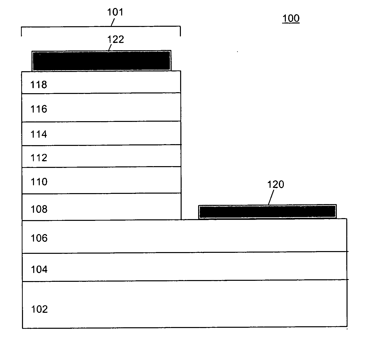
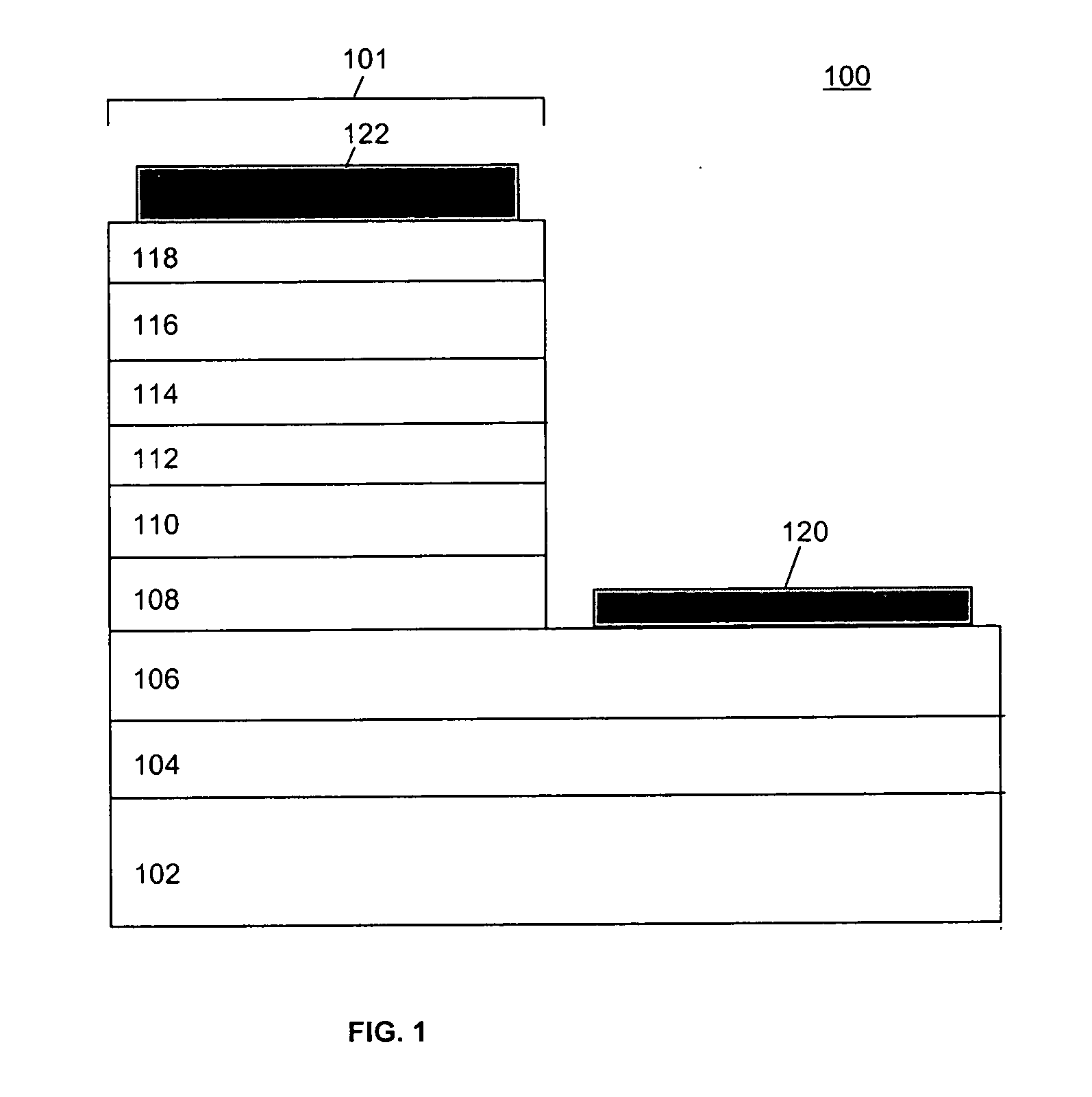
[0018] Turning now to FIG. 1, a sectional view of an edge emitting laser 100 is illu...


PUM


Abstract

Structures and methods for electronic devices with improved conductive regions are provided. The conductive region may include digital alloy superlattice structures, which allow higher doping levels to be achieved than for a bulk (random) alloy with the same average composition. Furthermore, the superlattice structures may improve the resistivity of the region, improving the current spreading of the region and hence the electronic properties of electronic devices such as optoelectronic devices.

Description

RELATED APPLICATION [0001] This application claims priority under 35 U.S.C. 119(e) from U.S. Provisional Application Ser. No. 60 / 579,639 filed 15 Jun. 2004, which application is incorporated herein by reference.GOVERNMENT FUNDING [0002] The invention described herein was made with government support under the following grant numbers, F496204-03-1-0437 (MDA / AFOSR). The United States Government may have certain rights in the invention.FIELD OF THE INVENTION [0003] This invention relates to electronic devices, in particular, to semiconductor devices. BACKGROUND OF THE INVENTION [0004] With the recent increased interest in mid-wavelength infrared (hereinafter referred to as “MWIR”) optoelectronic devices and applications, much attention has been directed to semiconductor optoelectronic devices, such as lasers, light emitting diodes (hereinafter referred to as “LEDs”), photodetectors, photodiodes, or the like. Particular concern has been directed to the area of lasers that operate at wav...

Claims


Application Information

Patent Timeline
IPC IPC(8): H01L33/00H01L33/30
CPCH01S5/20H01L33/305
Inventor HILL, PETER O.DAWSON, LARRY R.DOWD, PHILIPKRISHNA, SANJAY
Owner STC UNM
Why Eureka
Try Eureka