Light emitting diode and method of fabricating the same

a technology manufacturing methods, which is applied in the manufacture of semiconductor/solid-state devices, semiconductor devices, electrical devices, etc., can solve the problems of easy breakdown further deterioration of light emitting diodes, and degradation of internal quantum efficiency, so as to improve electrostatic discharge characteristics

Active Publication Date: 2012-02-16
SEOUL VIOSYS CO LTD
View PDF8 Cites 69 Cited by
  • Summary
  • Abstract
  • Description
  • Claims
  • Application Information

AI Technical Summary

Benefits of technology

[0016]Exemplary embodiments of the present invention provide a light

Problems solved by technology

When high voltage such as electrostatic discharge (ESD) is applied to the light emitting diode, ESD breakdown of the light emitting diode may easily occur due to the current concentration.
Since current may flow intensively through these thread dislocations, the ESD characteristics may lead to further deterioration of the light emitting diode.
This strain may cause a piezoelectric field in the quantum well layer, thereby leading to degradation of internal quantum efficiency.
However, the Si doping may have a negative effect on the crystal quality of the active region.
Further, due to the limitations of epitaxial growth technology, the multi-quantum well structure may be relatively thick according to the doping of Si.
In particular, when Si is doped in the active region including In, crystal defects may frequently occur on the surface of the active region and in the active region and a wavelength shift may be easily generated due to a space charge

Method used


Image

  • Light emitting diode and method of fabricating the same
  • Light emitting diode and method of fabricating the same
  • Light emitting diode and method of fabricating the same

Examples


experimental example 1

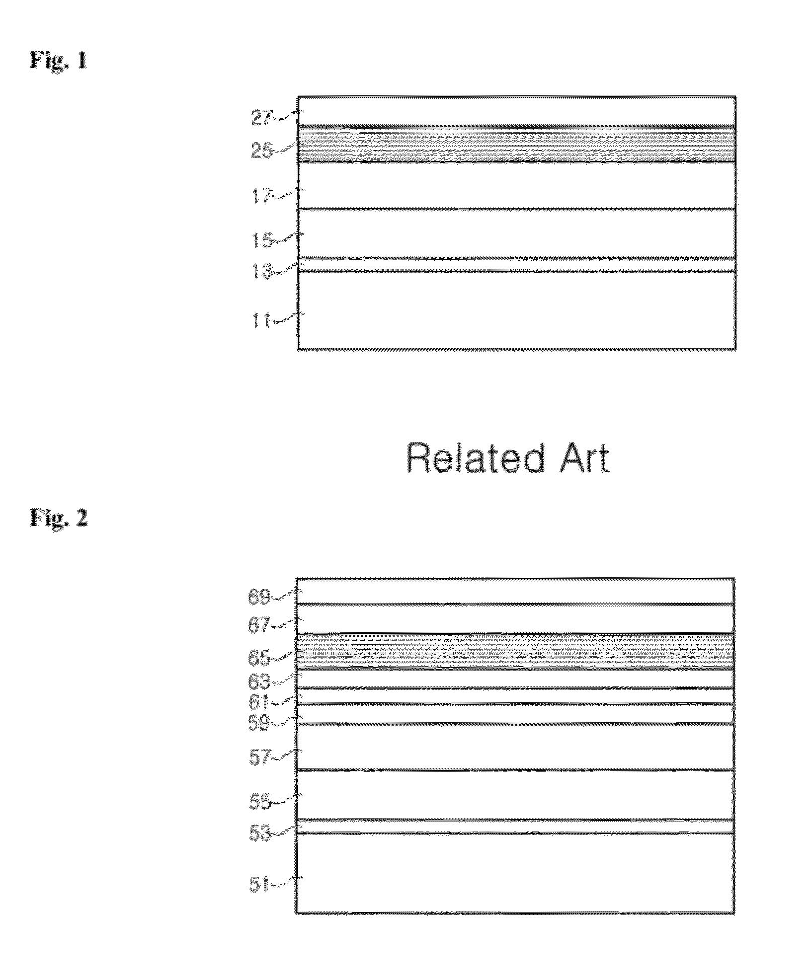
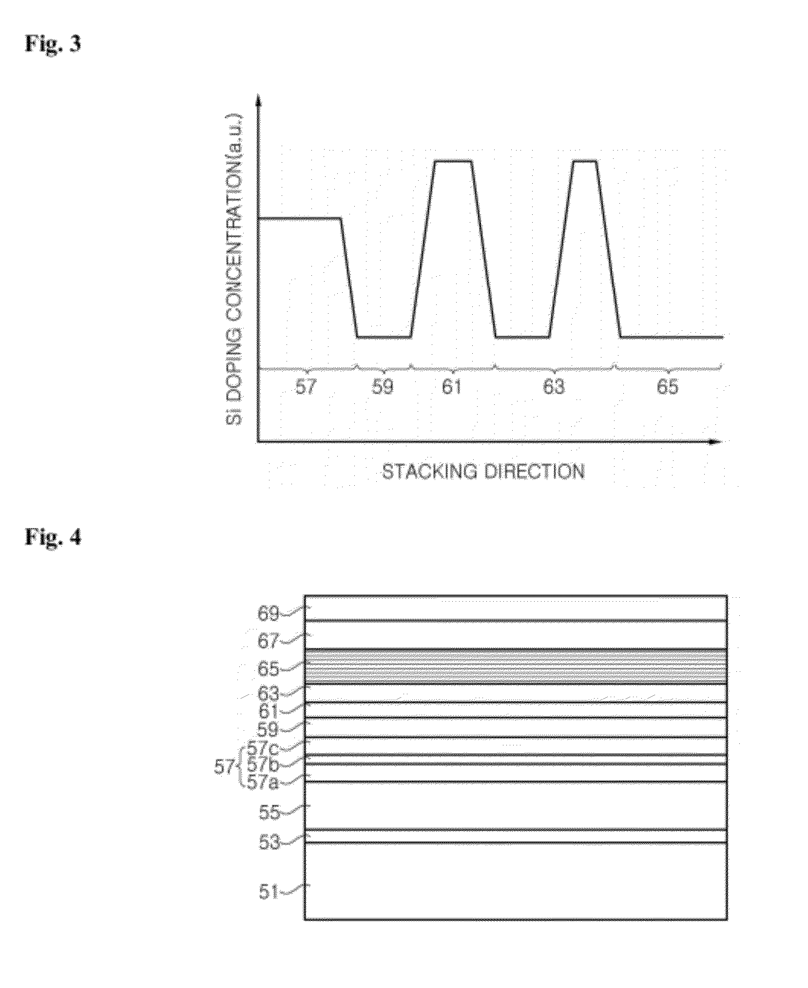
[0061]The epitaxial layers having the above-mentioned structure were grown with reference to FIG. 2 and FIG. 3 by using a metal-organic chemical vapor deposition (MOCVD) device. In the present experimental example, all the other conditions were the same as described above, and the Si doping position was different at the GaN / InGaN superlattice layer 63. The n-type GaN contact layer 57, the undoped GaN intermediate layer 59, the high-concentration doped GaN electron reinforcing layer 61 were sequentially grown on the undoped GaN buffer layer 55, the superlattice layer 63 was grown on the electron reinforcing layer 61, and the active region 65 having the multi-quantum well structure, the p-type AlGaN clad layer 67, and the p-type GaN contact layer 69 were sequentially grown on the superlattice layer 63.

[0062]In a Comparative Example, Si was doped on all of the GaN layers in the superlattice layer 63, and, in the Experimental Example 1, Si was doped only in the final layer of the superl...

experimental example 2

[0064]The light emitting diode having a structure according to the exemplary embodiment shown in FIG. 4 was grown by a MOCVD process. In the present exemplary embodiment, all the other conditions were the same as in the exemplary embodiment shown in FIG. 2, but the Comparative Example had an n-type contact layer 57 formed only n-type GaN while the Experimental Example 2 had an n-type contact layer 57 including n-type AlGaN layer interposed between n-type GaN layers.

[0065]The grown epitaxial layers were separated, together with the substrate, and the optical characteristics and the electrical characteristics were measured. The results are shown in Table 2. In this configuration, the ESD test was performed by applying a reverse voltage of 1000 V to functional light emitting diodes manufactured on the same wafer. Then, the failures of the light emitting diodes were checked, and the ESD characteristics were represented by an ESD pass ratio. The optical output and the leakage current wer...


PUM


Abstract

Exemplary embodiments of the present invention disclose a light emitting diode including an n-type contact layer doped with silicon, a p-type contact layer, an active region disposed between the n-type contact layer and the p-type contact layer, a superlattice layer disposed between the n-type contact layer and the active region, the superlattice layer including a plurality of layers, an undoped intermediate layer disposed between the superlattice layer and the n-type contact layer, and an electron reinforcing layer disposed between the undoped intermediate layer and the superlattice layer. Only a final layer of the superlattice layer closest to the active region is doped with silicon, and the silicon doping concentration of the final layer is higher than that of the n-type contact layer.

Description

CROSS-REFERENCE TO RELATED APPLICATIONS[0001]This application claims priority from and the benefit of Korean Patent Application No. 10-2010-0000559, filed on Jan. 5, 2010; Korean Patent Application No. 10-2010-0052860, filed on Jun. 4, 2010; Korean Patent Application No. 10-2010-0052861, filed on Jun. 4, 2010; and Korean Patent Application No. 10-2010-0113666, filed on Nov. 16, 2010, which are hereby incorporated by reference for all purposes as if fully set forth herein.BACKGROUND OF THE INVENTION[0002]1. Field of the Invention[0003]The present invention relates to a light emitting diode and a method of fabricating the same, and more particularly, to a light emitting diode with improved electrostatic discharge characteristics and / or luminous efficiency and a method of fabricating the same.[0004]2. Discussion of the Background[0005]Generally, a gallium nitride (GaN)-based semiconductor may be used for an ultraviolet or blue / green light emitting diode or laser diode, or the like, as ...

Claims


Application Information

Patent Timeline
IPC IPC(8): H01L33/04
CPCH01L21/02502H01L21/0254H01L21/02576H01L21/0262H01L33/007H01L33/06H01L33/04H01L33/32H01L21/0237H01L21/02458H01L33/0025H01L33/025
Inventor KIM, KWANG JOONGHAN, CHANG SUKYE, KYUNG HEECHOI, SEUNG KYUNAM, KI BUMKIM, NAM YOONKIM, KYUNG HAEYOON, JU HYUNG
Owner SEOUL VIOSYS CO LTD
Why Eureka
Try Eureka