Film temperature sensor and temperature sensing substrate

a temperature sensor and substrate technology, applied in the direction of positive temperature coefficient thermistors, instruments, heat measurement, etc., can solve the problems of affecting the temperature of the temperature sensing substrate and the deterioration of the cleanliness of the entire devi

Inactive Publication Date: 2006-02-16
KELK LTD
View PDF8 Cites 21 Cited by
  • Summary
  • Abstract
  • Description
  • Claims
  • Application Information

AI Technical Summary

Benefits of technology

[0013] A resistor pattern, which is formed from a zig-zag line of thin-film resistors possessing electrical resistance that changes in accordance with the temperature, can be employed in each of the above-mentioned plurality of thermal elements so as to cover a plurality of temperature measurement zones on the base film. A resistor pattern such as this can be formed on the base film using an etching, printing, sputtering or plating method. At the time this resistor pattern is formed, when R stands for a representative resistance value in the measurement temperature range of this resistor pattern, H stands for the dimension in the longitudinal direction of a temperature measurement zone, which this resistor pattern covers, T stands for the thickness of a resistance line thin-film, ρ stands for the electrical resistivity of a conductive material, A stands for the width of this resistance line, k stands for the ratio of the width of the space between adjacent resistance lines relative to the resistance line width A, and C stands for an arbitrarily selected coefficient, the width A of this resistance line can be selected from the range of
[0014] A film temperature sensor in accordance with the present invention can be used for the purpose of measuring temperatures in a semiconductor manufacturing process, and more particularly, for example, for the purpose of measuring the temperature distribution on the surface of a semiconductor wafer. In a film temperature sensor related to one embodiment for this purpose, this base film has the flat shape of a paddle. The head portion of this paddle-shaped base film is a circle, which is large enough to cover the entire area of the surface of either a semiconductor wafer or temperature-controlling stage, and is used in a state wherein it is either at

Problems solved by technology

However, when printing is used to pattern the sensor and lead on top of the temperature sensing substrate, since the lead terminal is on the wafer, this results in the need to link the lead terminal on the temperature sensing substrate to a wire lead.
Further, since there is a plurality of wire leads on top of the

Method used


Image

  • Film temperature sensor and temperature sensing substrate
  • Film temperature sensor and temperature sensing substrate
  • Film temperature sensor and temperature sensing substrate

Examples


first embodiment

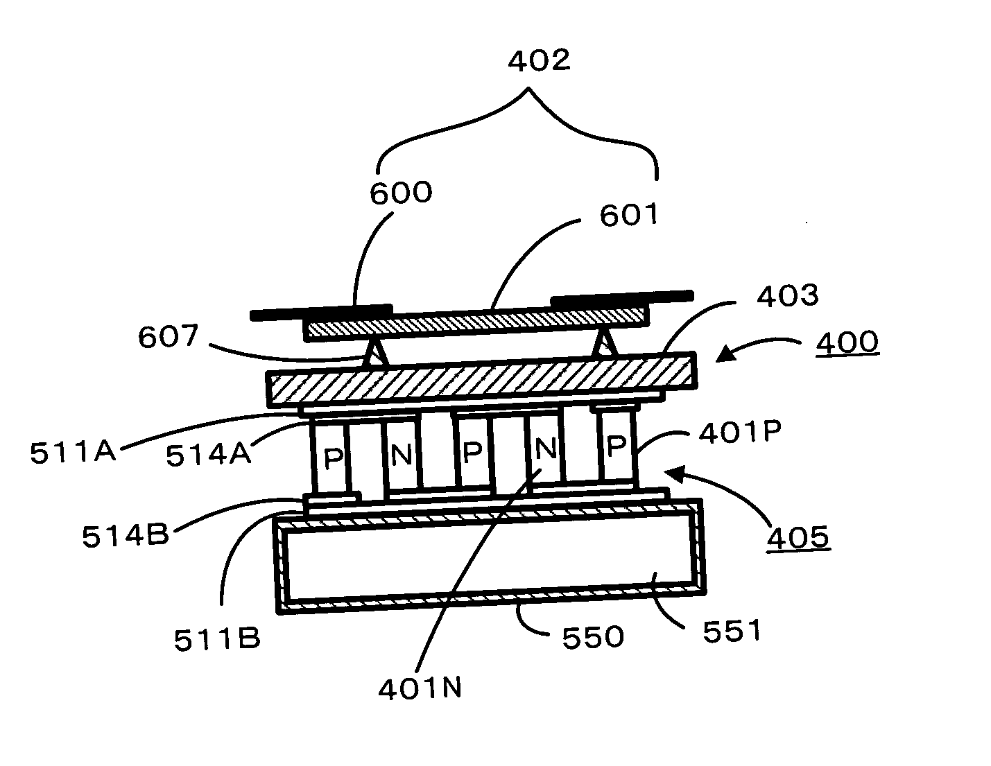
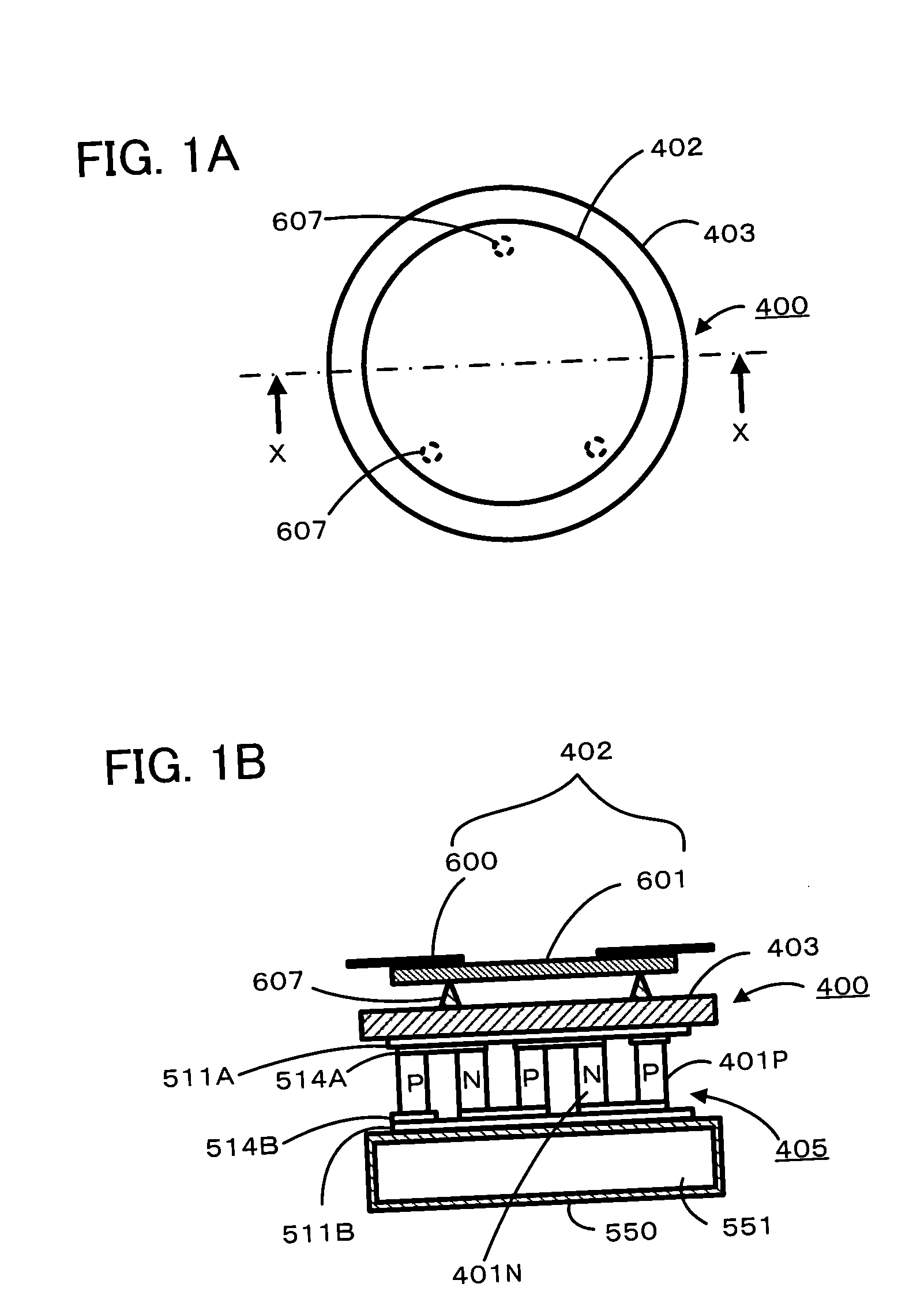
[0040] A temperature sensing substrate 402 according to the present invention is constituted from a semiconductor wafer 601 for use in measuring temperature, having the same specifications as a to-be-processed semiconductor wafer used in a semiconductor manufacturing process; and one or more film-shaped temperature sensors (hereinafter, called a film temperature sensor) 600, which are respectively applied to one or more locations (ordinarily, several locations or more) where the temperature on the surface of this semiconductor wafer 601 should be measured.

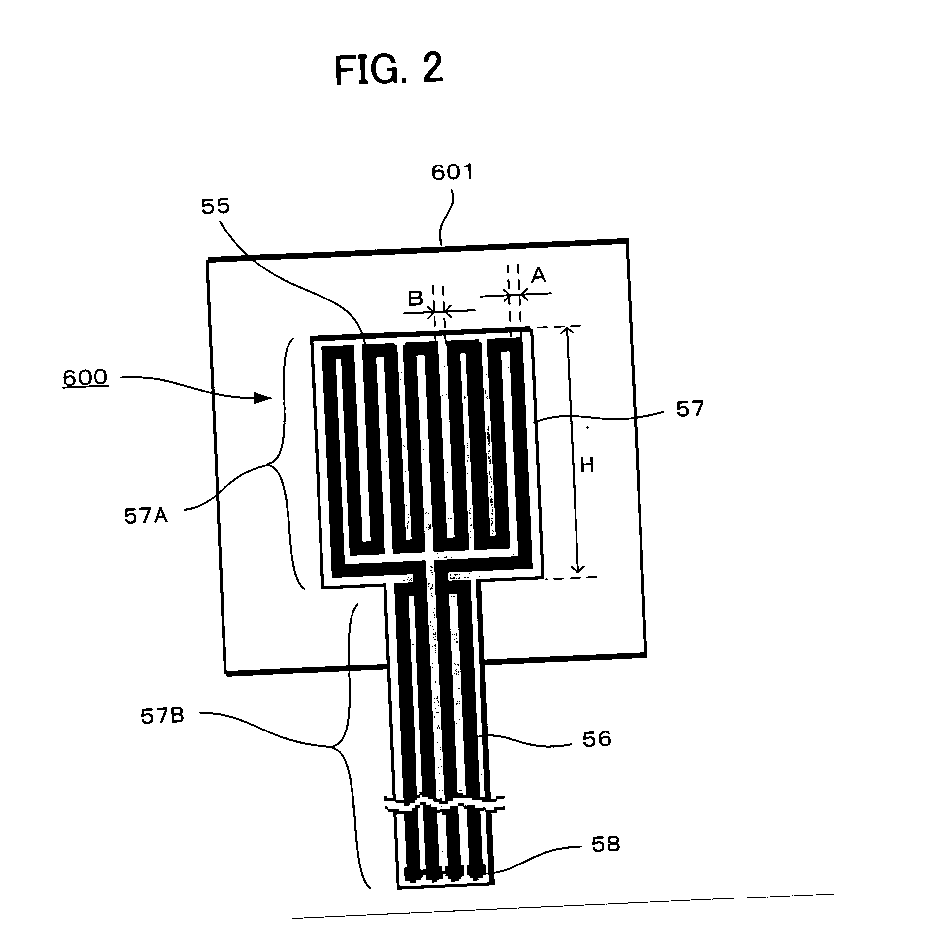
[0041] The film temperature sensor 600, as will be explained below, comprises a base film made of a flexible insulating material; one or more thin-film thermal elements for measuring temperature; a plurality of terminals for outputting to the outside as electrical signals the temperature data detected by this thermal element; and a plurality of thin-film leads for transferring to the terminals the electrical signals from the therma...

second embodiment

[0073]FIG. 11 is an illustration showing a manufacturing method for a film temperature sensor 600.

[0074] As shown in FIG. 11, after the method shown in FIG. 10 has been carried out, in addition, a cover lay 701 of the same paddle shape as the base film 57 is laminated onto the surface of the side of the base film 57 on which the resistor pattern 55 and lead 56 are formed.

[0075] The cover lay 701 has the function of insulating, rust-proofing and mechanically protecting the resistor pattern 55 and lead 56. As the cover lay 701 material, a film-like resin having an adhesive or an adhesive layer, a liquid resin, such as polyimide or varnish, solder resist, a photosensitive resin, or plating can be used. When a film-like resin is used as the cover lay 701, both a denatured layer like a denatured polyimide, and an adhesive layer like a polyimide, polyethylene, or PET can be used. Then, methods for mounting a cover lay 701 using these materials include heat processing, printing, electrode...

third embodiment

[0076]FIG. 12 is an illustration showing a manufacturing method for a film temperature sensor 600.

[0077] As shown in FIG. 12, when the cover lay 701 is laminated to the base film 57 using the method shown in FIG. 11, an adhesive sheet 702 is sandwiched between the two, and these three are laminated together.

[0078] A resin-based adhesive sheet and an adhesive can be used in the adhesive sheet 702, examples of this type of sheet being a polyimide-, epoxy-, silicon-, or acrylic-based sheet. These three are then laminated in the order of base film 57, adhesive sheet 702, and cover lay 701, and subjected to heat and pressure treatments to produce s film temperature sensor 600. Furthermore, the adhesive sheet 702 does not necessarily have to be in the form of a sheet, but rather can be replaced by a liquid that is coated onto the adhesive object.


PUM


Abstract

A film-like temperature sensor for more accurately measuring the temperatures at plural locations on the surface of a semiconductor wafer comprises a base film made of an insulating material; plural thin-film thermal elements for sensing temperature; plural thin-film leads, connected to the thermal elements; and plural thin-film terminals connected to the ends of the leads. The thermal elements, leads, and terminals are integrally formed either on the surface or in the thickness of the base film. The base film has a flat shape like a paddle, and comprises a head portion to be attached to the surface of a semiconductor wafer, and a strip-shaped tail portion extending outwardly of the semiconductor wafer. The plural thermal elements are arranged on the head portion in the form of either a concentric circle, spiral, matrix, or raster, and the plural terminals are arranged on the tail portion.

Description

CROSS-REFERENCE TO PRIOR APPLICATION [0001] This application relates to and claims priority from Japanese Patent Application No. 2004-235505, filed on Aug. 12, 2004, the entire disclosure of which is incorporated herein by reference. [0002] 1. Field of the Invention [0003] The present invention relates to a temperature sensor and temperature sensing substrate useful for measuring either the temperature of a semiconductor wafer or other such substrate, or the temperature of a temperature-controlling stage for heating and cooling such a substrate. [0004] 2. Background of the Invention [0005] For example, in the manufacturing process for a semiconductor product, a semiconductor wafer is placed on a temperature-controlling stage, which has heating and cooling capabilities, and processing, such as applying a coating of photoresist material to this semiconductor wafer, and subsequently subjecting it to etching, is carried out while adjusting the temperature of the semiconductor wafer usin...

Claims


Application Information

Patent Timeline
IPC IPC(8): G01K7/00
CPCG01K7/00G01K1/026
Inventor SAIO, KATSUOOHSAWA, AKIHIRO
Owner KELK LTD
Why Eureka
Try Eureka