Universal and integrated wafer testing real-time monitoring software system and its open system architecture

Inactive Publication Date: 2006-02-16
CHEN WEN LING +1
View PDF1 Cites 25 Cited by
  • Summary
  • Abstract
  • Description
  • Claims
  • Application Information

AI Technical Summary

Benefits of technology

[0028] Another major characteristic of this invention is that multiple workstations can process data from probers simultaneously. The on-line monitor on a production line can see production results from multiple major workstations through the network drive and drive mapping functions. After which it can take the next processing step, which is to re-generate a raw data floppy diskette depending on whether a retest or a fail die retest is necessary. This greatly reduces cycle time of wafer testing. This invention also has a multi-processing function. As a result it can minimize risks of data loss. It also has a built-in intelligence function, so upgrading of any of the four programs does not affect data communication between them.
[00

Problems solved by technology

Users cannot find the root cause of low yield wafers from the database because most of them are binary files and show no relationship.
Besides, it provides no E test data or ASCII file to users, therefore, it is difficult to trace wafer process errors.
Due to marketing considerations, software from one prober vendor does not support reading binary file types of another vendor.
Furthermore users easily subject themselves to pressure from vendors, such as they should only buy one type of prober.
Additionally, they cannot generate good competi

Method used


Image

  • Universal and integrated wafer testing real-time monitoring software system and its open system architecture
  • Universal and integrated wafer testing real-time monitoring software system and its open system architecture
  • Universal and integrated wafer testing real-time monitoring software system and its open system architecture

Examples


Embodiment Construction

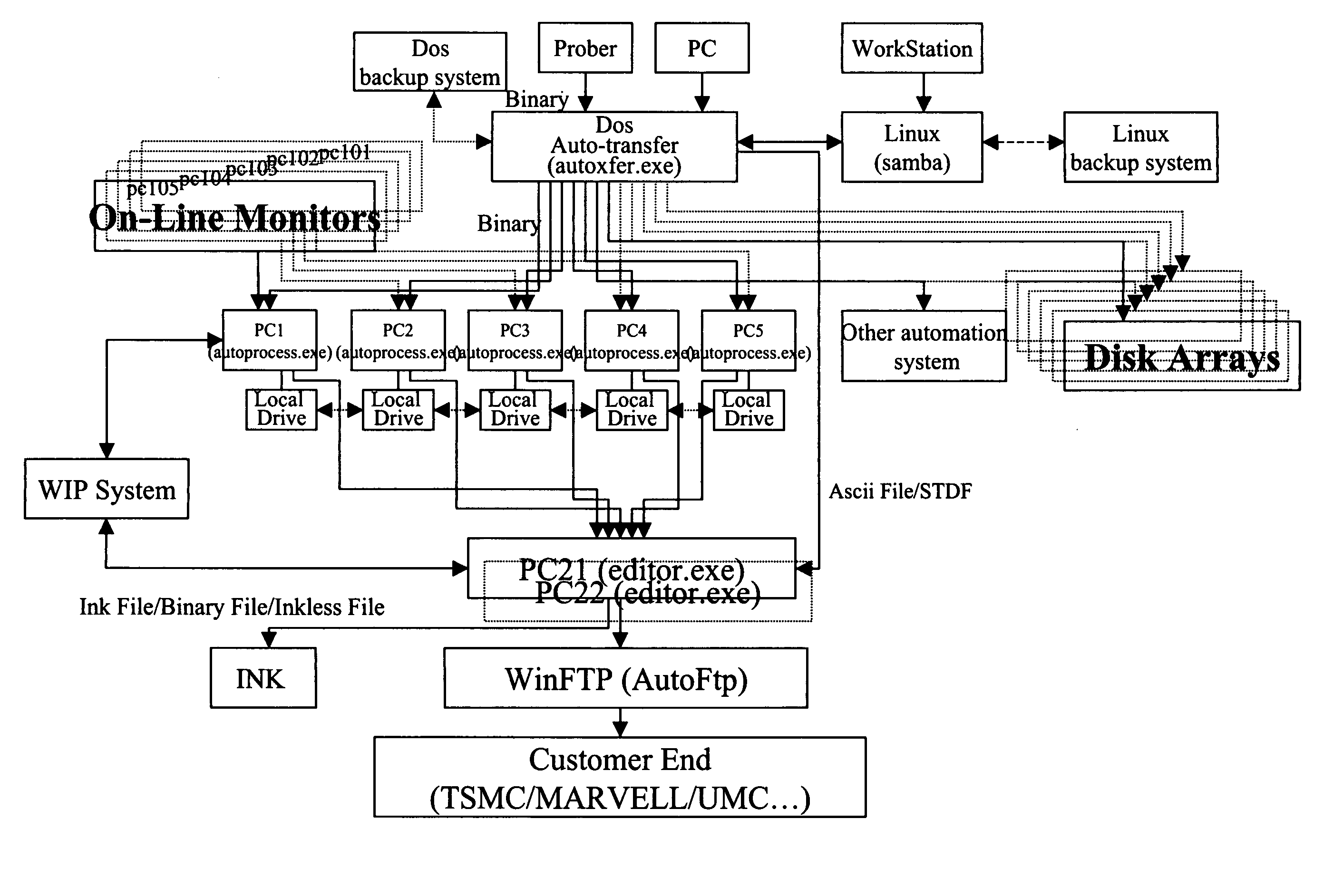
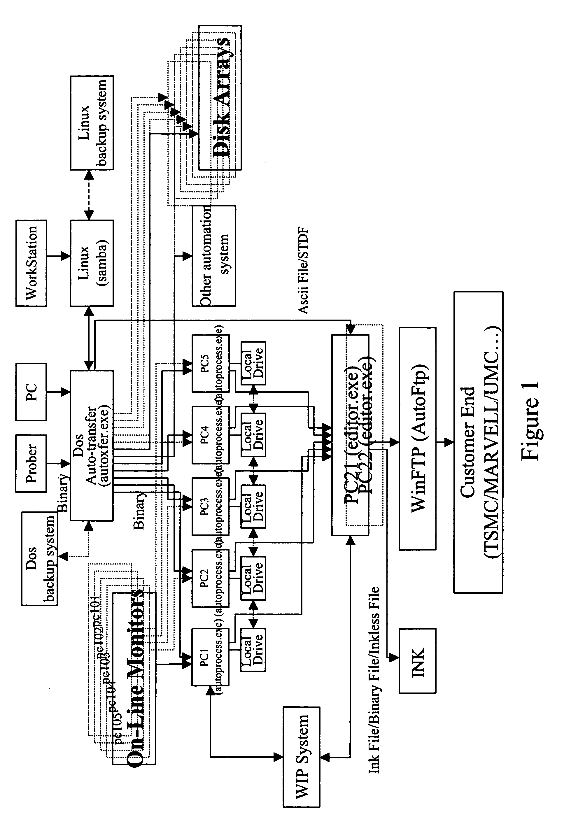
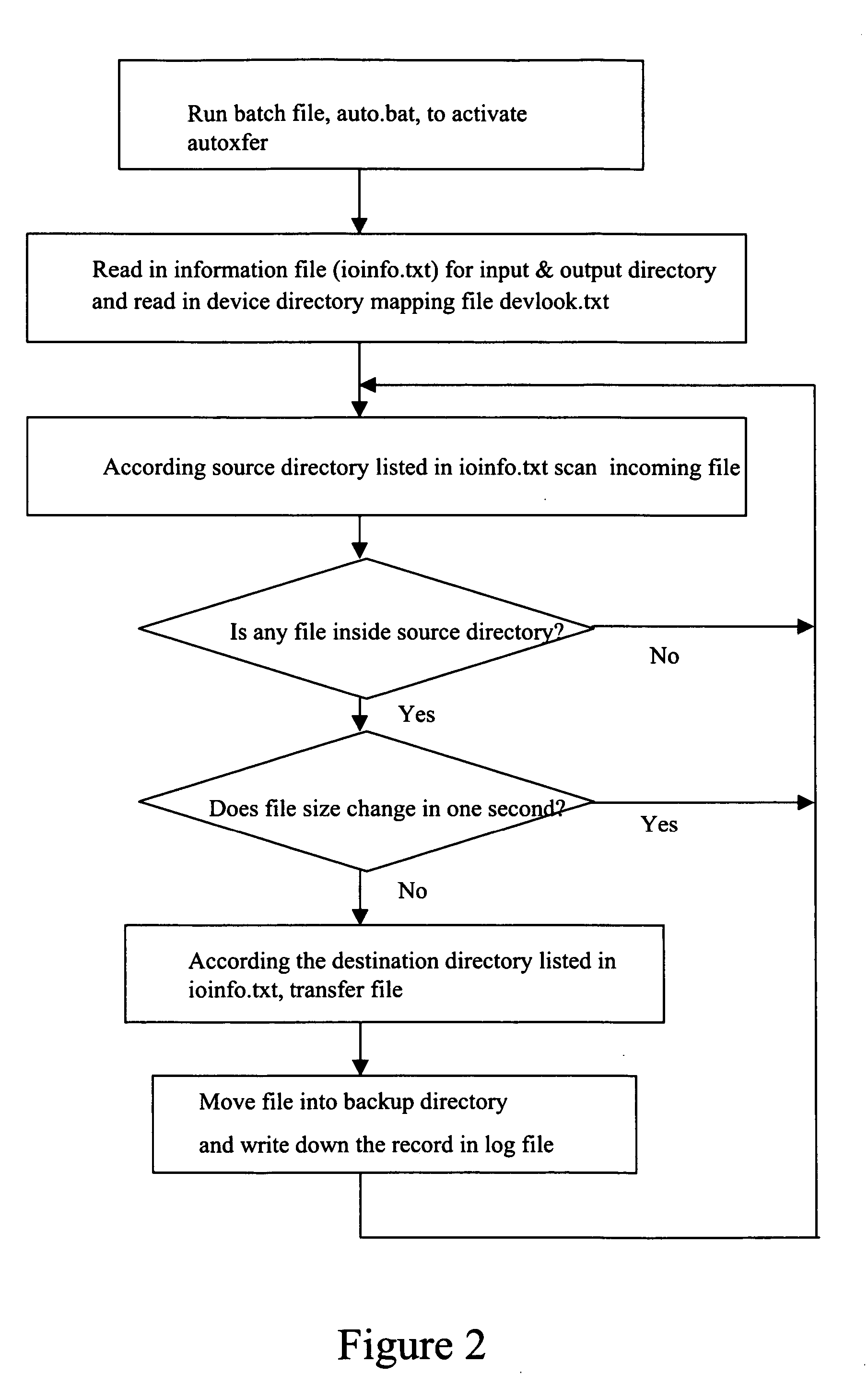
[0100] Reference will now be made in detail to the preferred embodiments of the present invention, examples of which are illustrated in the accompanying drawings. Wherever possible, the same reference numbers are used in the drawings and the description to refer to the same or like parts.

[0101] Regarding this invention, all detailed explanations on the software specification are described in the following software description of functionality and capability.

Conventions:

[0102] This documentation uses the following typographic conventions:

ExampleDescription[option]Items inside single square brackets are optional.{1|2}Braces and a vertical bar indicate a choice amongtwo or more items. You must choose one andonly one of these items.[option . . .]Three dots (an ellipsis) following an item indicatethat more items having the same form may appear.EdaDataBold type indicates keyword or word that mustbe spelled exactly as shown except the case,which is insensitive.netdriveWords in italic...


PUM


Abstract

A wafer testing real-time monitoring software system and its unique open software architecture which achieves real-time monitoring of wafer test results and on-line changing of externally hooked software to satisfy customer needs without changing its main program. The software structure receives and processes binary files from different probers and converts these into readable ASCII files. The system consists of four software programs that can operate independently. These programs are an automatic transfer program, a program which converts wafer test results from a binary file to an ASCII file, a program which receives the ASCII files and performs wafer map editing, and an auto-ftp program which automatically scans data and sends data to remote locations. Additionally, multiple workstations can process data from probers simultaneously. The on-line monitor on a production line can see production results from multiple major workstations through the network drive and drive mapping functions.

Description

BACKGROUND OF THE INVENTION [0001] 1. Field of the Invention [0002] The present invention relates to testing software. More specifically, the present invention discloses a universal and integrated wafer testing real-time monitoring software system and its open system architecture. [0003] 2. Description of the Prior Art [0004] Wafer testing is an extremely important link in the semiconductor industry. However, the testing results need to be analyzed very quickly in order to improve yield. Common programs only provide a database to users from a graphical user interface (GUI). Users cannot find the root cause of low yield wafers from the database because most of them are binary files and show no relationship. Besides, it provides no E test data or ASCII file to users, therefore, it is difficult to trace wafer process errors. Yield improvement is related to wafer manufacturing processes and IC design specifications, but the present invention can perform numerous sorts of analyses to fin...

Claims


Application Information

Patent Timeline
IPC IPC(8): G01M19/00G01M99/00
CPCG01R31/318511G01R31/31718
Inventor CHEN, WEN-LINGWEI, MING
Owner CHEN WEN LING
Why Eureka
Try Eureka