Magnetic memory adopting synthetic antiferromagnet as free magnetic layer

a technology of magnetic memory and free layer, applied in the field of magnetic memories, can solve problems such as uncertainty of magnetization directions, and achieve the effect of improving the operation range of magnetic memories

Active Publication Date: 2006-02-23
NEC CORP
View PDF7 Cites 58 Cited by
  • Summary
  • Abstract
  • Description
  • Claims
  • Application Information

AI Technical Summary

Benefits of technology

[0019] Therefore, an object of the present invention is to improve

Problems solved by technology

This causes uncertainty of the directions of the magnetizations after the r

Method used


Image

  • Magnetic memory adopting synthetic antiferromagnet as free magnetic layer
  • Magnetic memory adopting synthetic antiferromagnet as free magnetic layer
  • Magnetic memory adopting synthetic antiferromagnet as free magnetic layer

Examples


first embodiment

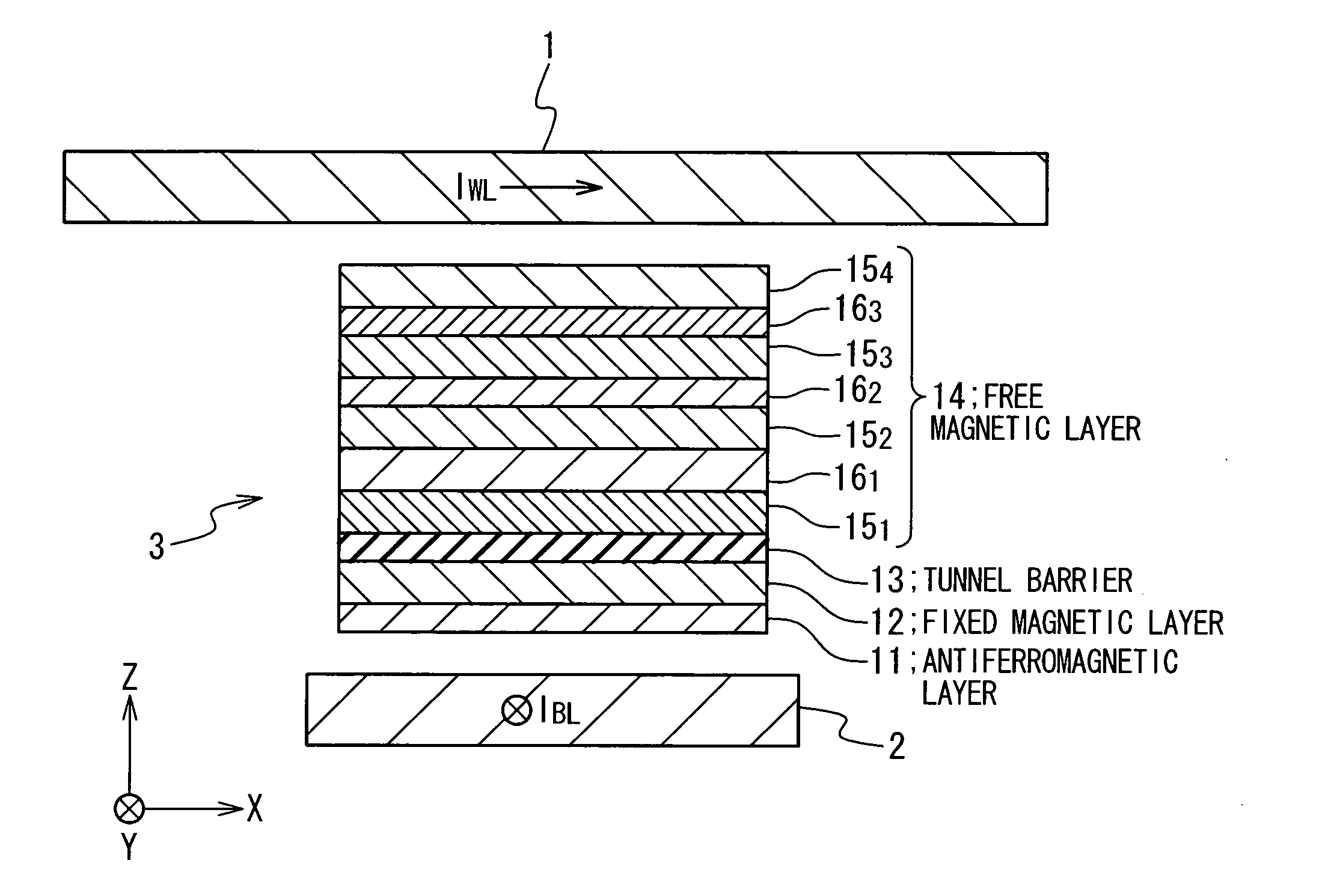
[0047]FIG. 6 is a section view illustrating an exemplary structure of a magnetic memory in a first embodiment of the present invention. The magnetic memory is composed of a word line 1, a bit line 2, and a magnetoresistance element 3, used as a memory cell. It will be understood that FIG. 6 partially illustrates the structure of the magnetic memory, and the magnetic memory is actually composed of a number of word lines 1, bit lines 2, and magnetoresistance elements 3. The word line 1 and the bit line 2 are extended in substantially orthogonal directions; in this embodiment, an x-axis direction is defined along the word line 1, and a y-axis direction is defined along the bit line 2. The word line 1 and the bit line 2 are connected to a write circuit (not shown) that provides a set of write currents IWL and IBL for the word line 1 and the bit line 2, respectively. In one embodiment, the write circuit is composed of decoders, and current sources developing the write currents IWL and IB...

second embodiment

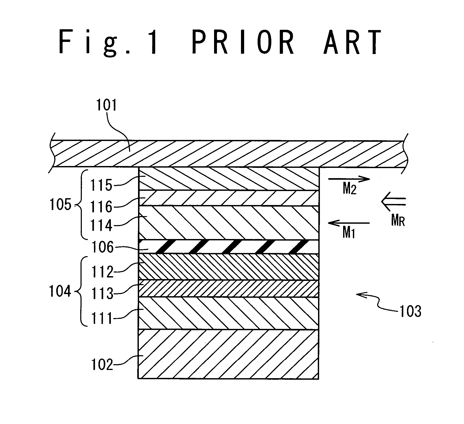
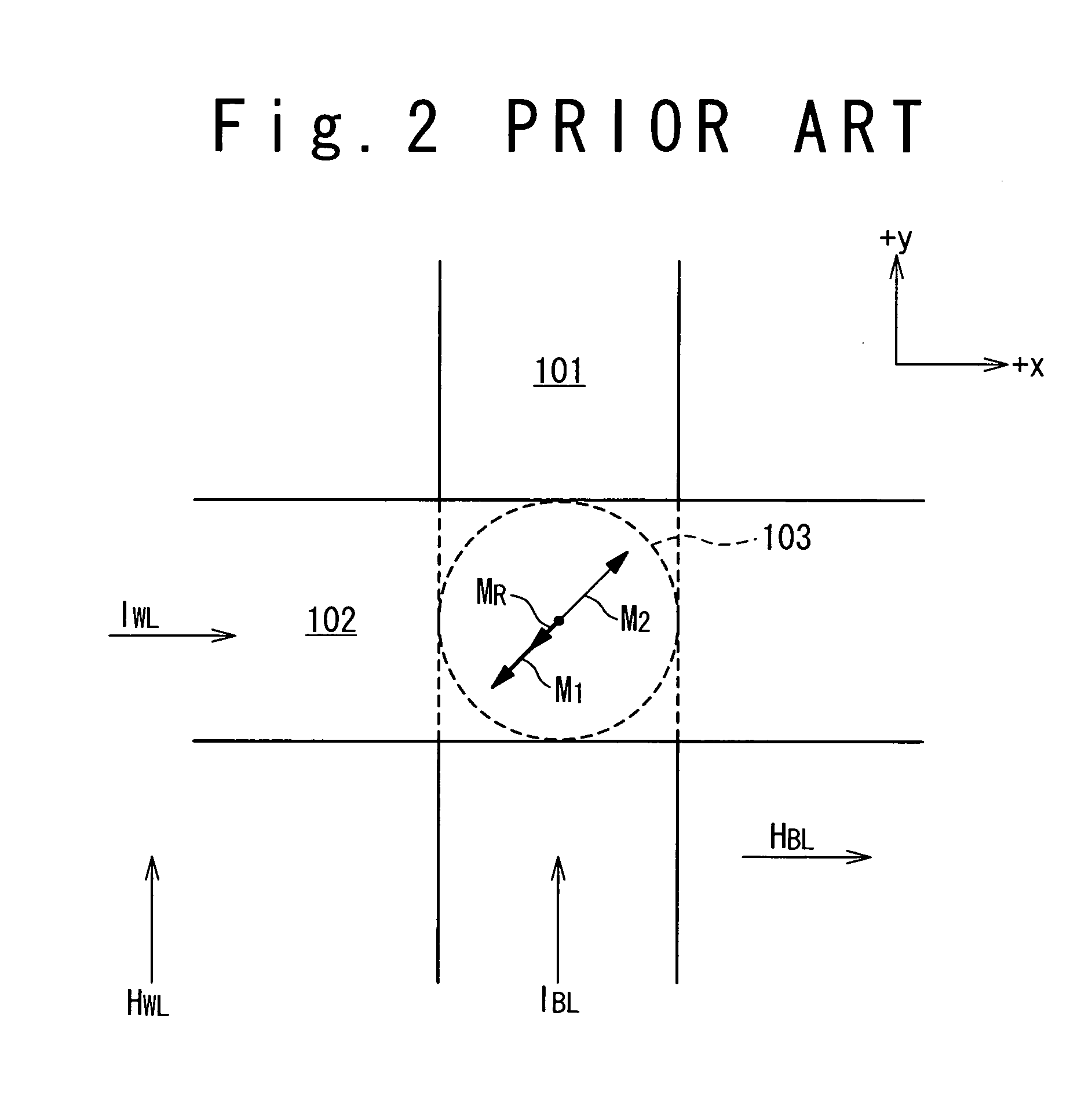
[0077] As described above with reference to FIG. 9B, the magnetic memory presented in the first embodiment may suffer from the fact that he ferromagnetic layers 151 to 154 do not function as a synthetic antiferromagnet due to the independent behavior of the ferromagnetic layer 151 from the remaining ferromagnetic layers 152 to 154, when the strength of the antiferromagnetic coupling between the ferromagnetic layer 151 and 152 is largely different from those between the ferromagnetic layer 152 and 153 and between the ferromagnetic layer 153 and 154. This undesirably inhibits the magnetic memory from achieving successful toggle writing.

[0078] In order to avoid such problem, the free magnetic layer is desirably designed so that the intermediate pair(s) of the ferromagnetic layers exhibit relatively strong antiferromagnetic coupling compared to the both end pairs of the ferromagnetic layers.

[0079]FIG. 16 is a section view illustrating an exemplary structure of such designed magnetic m...


PUM


Abstract

A magnetic memory is composed of: a magnetoresistance element including a free magnetic layer; a first interconnection extending in a first direction obliquely to an easy axis of the free magnetic layer; a second interconnection extending in a second direction substantially orthogonal to the first direction; and a write circuit writing data into the free magnetic layer through developing a first write current on the first interconnection, and then developing a second write current on the second interconnection with the first write current turned on. The free magnetic layer includes: first to N-th ferromagnetic layers and first to (N−1)-th non-magnetic layers with N being equal to or more than 4, the i-th non-magnetic layer being disposed between the i-th and (i+1)-th ferromagnetic layers with i being any of natural numbers equal to or less than N−1. The free magnetic layer is designed so that antiferromagnetic coupling(s) between the j-th and (j+1)-th ferromagnetic layers is stronger than that between the first and second ferromagnetic layers, j being any of integers ranging from 2 to N−2.

Description

BACKGROUND OF THE INVENTION [0001] 1. Field of the Invention [0002] The present invention relates to magnetic memories, more particularly to magnetic memories incorporating synthetic antiferromagnet free layers that are composed of multiple ferromagnetic layers separated by non-magnetic layers. [0003] 2. Description of the Related Art [0004] The magnetic memory (MRAM) is one of the promising non-volatile semiconductor storage devices. A memory cell of the magnetic memory is typically composed of a magnetoresistance element including a fixed magnetic layer and a free magnetic layer separated by a spacer layer; data is stored as the direction of the magnetization of the free magnetic layer. Reading data from a memory cell is achieved on the basis of the change in the resistance of the magnetoresistance element resulting from the tunneling magnetoresistance (TMR) effect or the Giant magnetoresistance (GMR) effect. A thin insulating layer is used as the spacer layer for a magnetic memor...

Claims


Application Information

Patent Timeline
IPC IPC(8): H01L29/94
CPCB82Y25/00G11C11/16H01L43/08H01F10/3272H01F10/3254H10N50/10
Inventor MORI, KAORUSUZUKI, TETSUHIROFUKUMOTO, YOSHIYUKIMIURA, SADAHIKO
Owner NEC CORP
Why Eureka
Try Eureka