Multiple power density chip structure

a chip structure and power density technology, applied in the direction of semiconductor devices, electrical equipment, semiconductor/solid-state device details, etc., can solve the problems of increasing power density, limiting the further increase of system performance, and the ability to adequately cool the chips, so as to achieve lower thermal resistance and higher thermal resistance

Inactive Publication Date: 2006-02-23
GLOBALFOUNDRIES INC
View PDF19 Cites 28 Cited by
  • Summary
  • Abstract
  • Description
  • Claims
  • Application Information

AI Technical Summary

Benefits of technology

[0017] In another embodiment of the invention a compliant thermal adhesive layer material is used on a lower power density semiconductor device and a rigid thermal adhesive layer material is used on a high power density device. The heat spreader may be the cap or lid of the package and a heat sink may be subsequently attached to heat spreader.
[0018] In another aspect of the invention there is disclosed a method for cooling multiple semiconductor devices with different cooling requirements on a common chip carrier with a common lid or heat spreader comprising

Problems solved by technology

The problem of heat removal becomes more difficult as chip geometries are scaled down and operating speeds are increased, resulting in increased power density.
The ability to adequately cool the chips can therefore be a limiting factor in the further increase of system performance.
Integrated circuit chips mounted face down on wiring substrates, and particularly multiple chips on a common substrate such as is found in a multichip module (MCM), present special cooling difficulties.
An additional problem is that processor chips, and other chips, frequently have a “hot spot” which can have a heat flux (W/cm2) significantly greater than the average heat flux resulting in temperatures approxim

Method used


Image

  • Multiple power density chip structure
  • Multiple power density chip structure
  • Multiple power density chip structure

Examples


Embodiment Construction

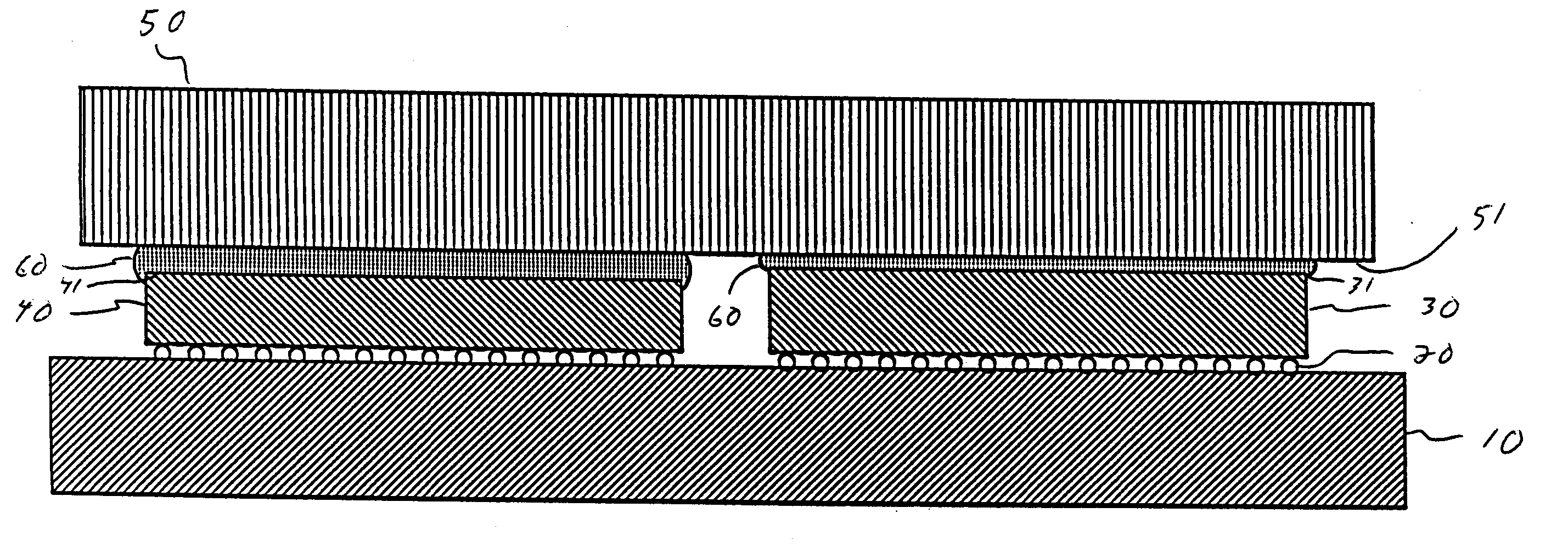
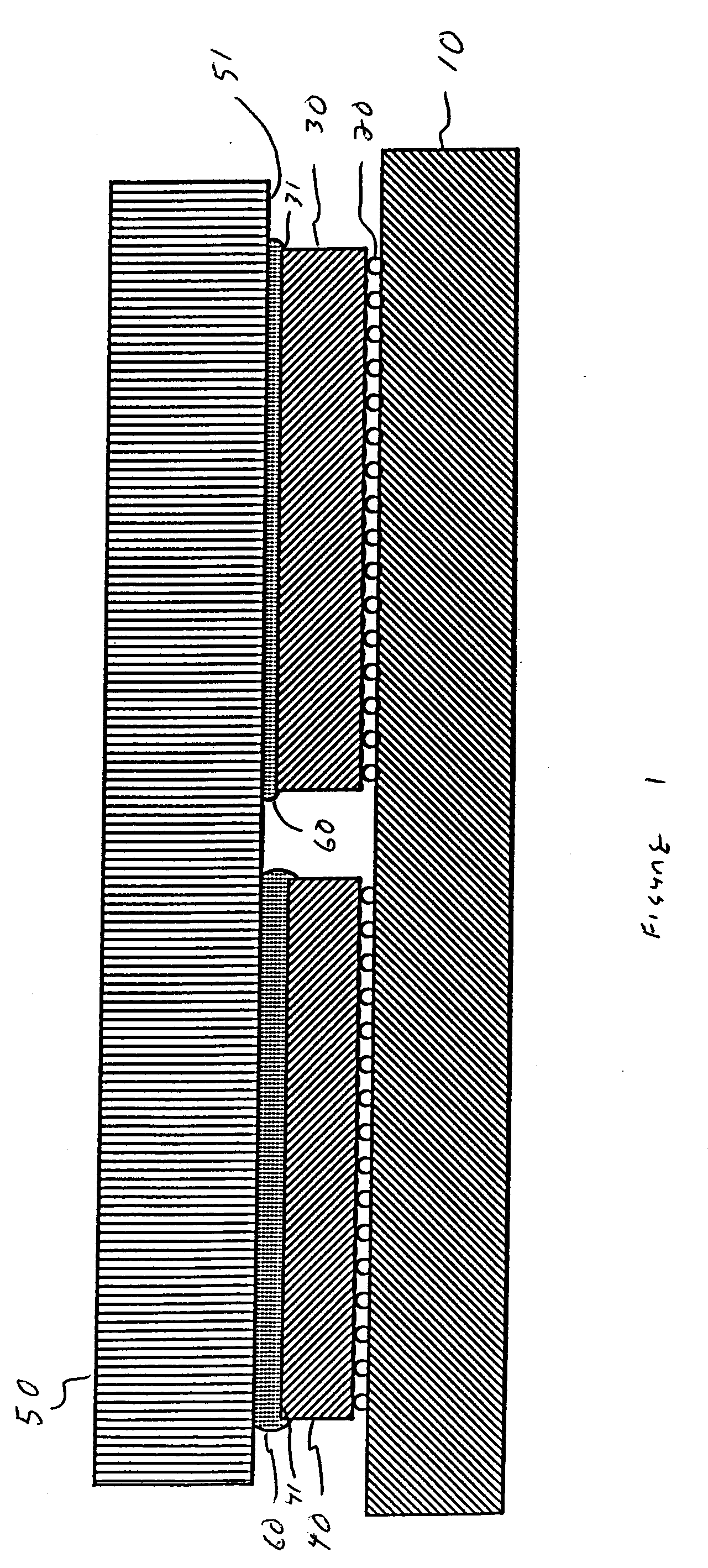
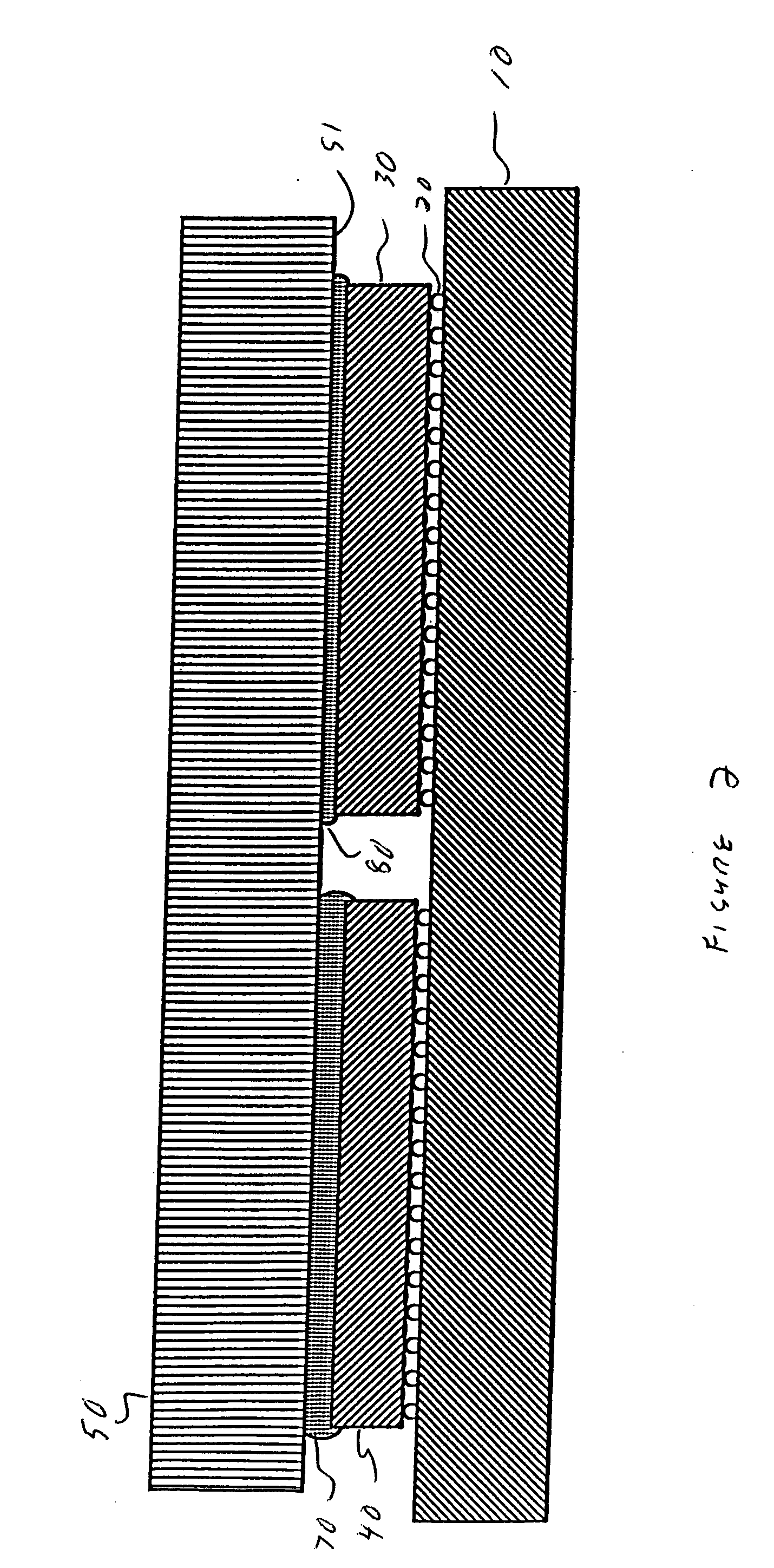
[0023] In a first embodiment of the invention, the lower power density devices which will be mounted on a common wiring substrate or chip carrier (first level package) and share a thermal spreader with a higher power density device, or a device which requires a lower total thermal resistance, are thinned, preferably at the wafer level, to insure that after all the devices are mounted onto the common wiring substrate, the higher power density device will project above all lower power density devices. As previously mentioned, when multiple devices are attached face down to a common wiring substrate, such as with solder balls (C4's), the typical device to device height variation is about + / −20 microns, though will of course vary depending on the type of wiring substrate used, the type of electrical attachment to the wiring substrate, the initial specifications on the wafers, and the wafer processing.

[0024] As an example, if the + / −20 micron variation mentioned above is a one sigma val...


PUM


Abstract

A multiple power density packaging structure with two or more semiconductor chips on a common wiring substrate having a common thermal spreader with a planar surface in thermal contact with the non-active surfaces of the chips. The semiconductor chips have different cooling requirements and some of the chips are thinned to insure that the chips requiring the lowest thermal resistance has the thinnest layer of a thermal adhesive or metal or solder interface between the chip and thermal spreader.

Description

BACKGROUND OF INVENTION [0001] The present invention relates to the cooling of integrated circuit (IC) packaging structures. More particularly the present invention is directed to the cooling of multiple chips, or ICs, using a common heat spreader or lid structure where the chips have different cooling requirements. [0002] As heat is generated during the functioning of integrated circuit chips (ICs), the thermal resistance to the heat sink must be small so that the operating temperature of the chip is low enough to assure the continued reliable operation of the device. The problem of heat removal becomes more difficult as chip geometries are scaled down and operating speeds are increased, resulting in increased power density. The ability to adequately cool the chips can therefore be a limiting factor in the further increase of system performance. Integrated circuit chips mounted face down on wiring substrates, and particularly multiple chips on a common substrate such as is found in...

Claims


Application Information

Patent Timeline
IPC IPC(8): H01L21/50H01L23/34
CPCH01L23/36H01L23/3735H01L25/0655H01L23/42H01L2224/73253H01L23/3732H01L23/3738H01L2224/16H01L2924/00011H01L2924/00014H01L2224/0401
Inventor COLGAN, EVAN G.KATOPIS, GEORGE A.RAMASWAMY, CHANDRASHEKHARSTOLLER, HERBERT I.
Owner GLOBALFOUNDRIES INC
Why Eureka
Try Eureka