Semiconductor device
a semiconductor device and semiconductor technology, applied in the field of semiconductor devices, can solve the problems of more prone to cracking at the interface of insulating films, and achieve the effect of minimizing the impact to associated regions and suppressing the propagation of cracks in semiconductor devices
- Summary
- Abstract
- Description
- Claims
- Application Information
AI Technical Summary
Benefits of technology
Problems solved by technology
Method used
Image

Examples
first embodiment
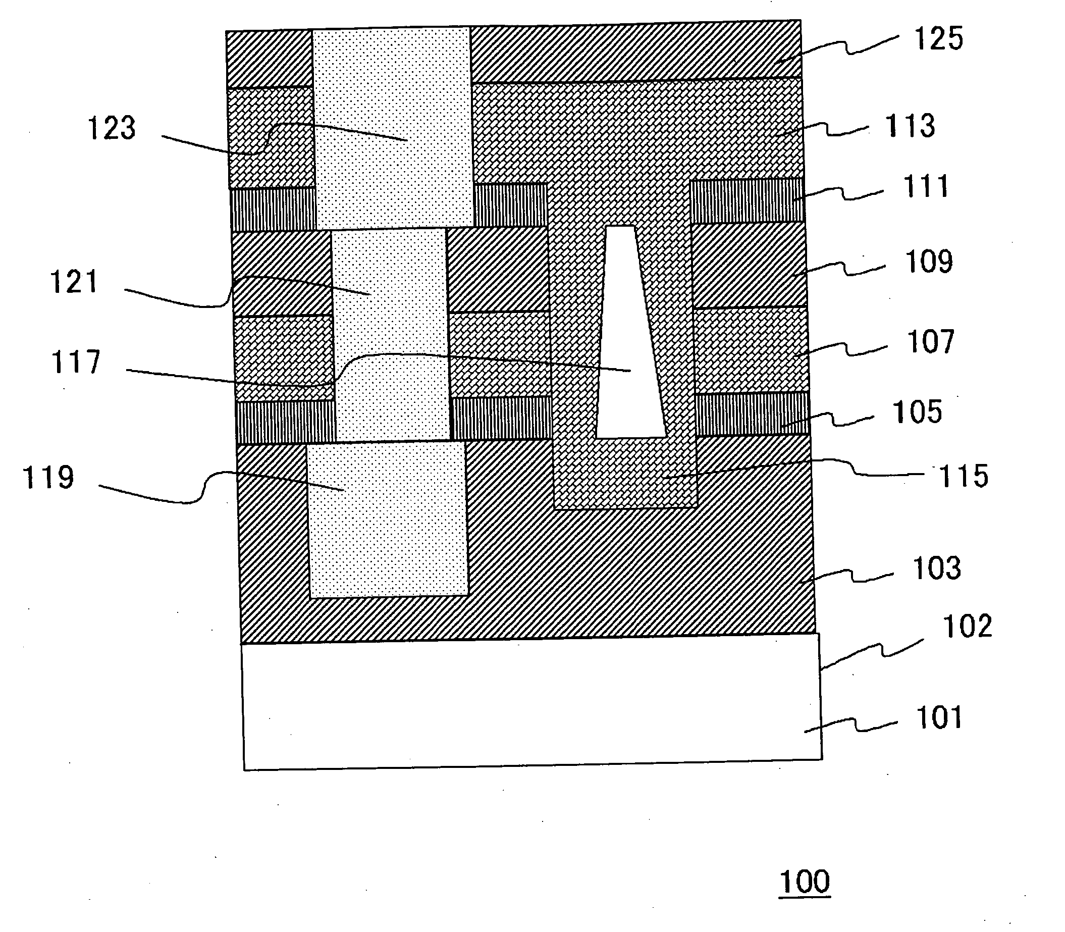
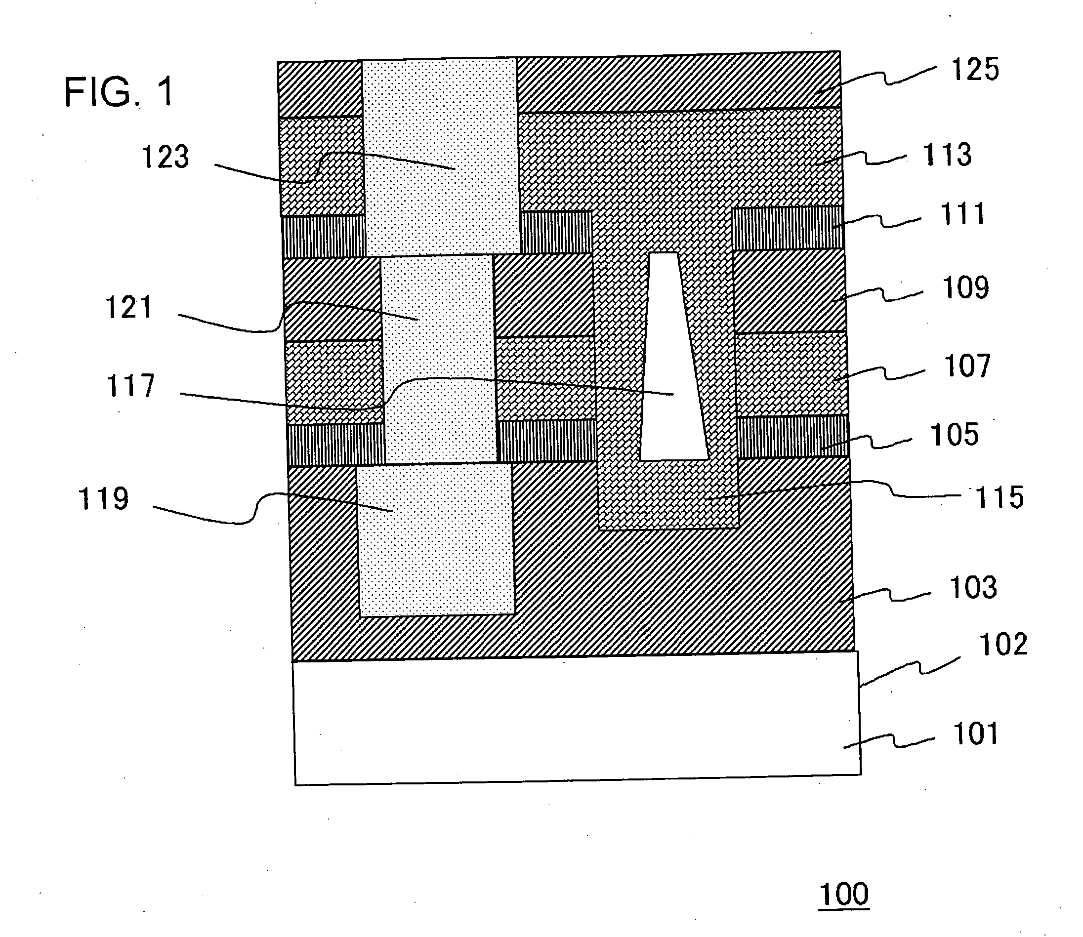
[0057] A first embodiment relates to a semiconductor device including a multilayer interconnect structure in which a low dielectric constant film is employed as an insulating interlayer.
[0058]FIG. 1 is a schematic cross-sectional view showing a configuration of a semiconductor device according to the present embodiment. Referring to FIG. 1, the semiconductor device 100 includes an insulating interlayer formed on a silicon substrate, and the insulating interlayer includes a multilayer interconnect structure including a copper interconnect and a via. The structure illustrated in FIG. 1 represents a portion of such a multilayer interconnect structure formed through a single damascene process, in which a lower interconnect constituted of a Cu film 119 is connected to an upper interconnect constituted of a Cu film 123 via a Cu plug 121.
[0059] The lower interconnect constituted of the Cu film 119 is located inside the insulating film 103. The insulating film 103 is constituted of stacke...
second embodiment
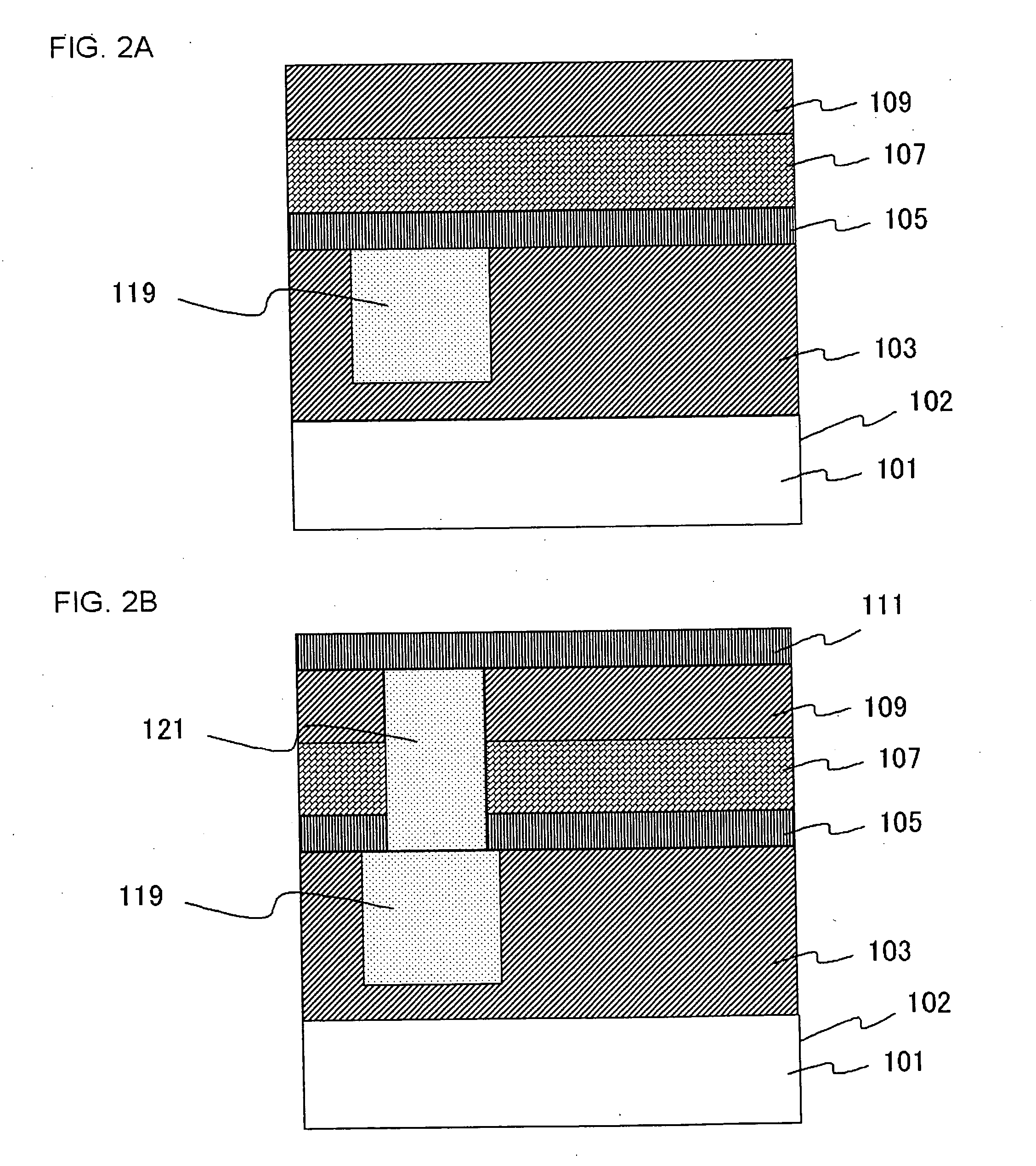
[0106]FIG. 15 is a schematic cross-sectional view showing a configuration of a semiconductor device according to a present embodiment of the present invention. The semiconductor device 110 shown in FIG. 15 includes an interconnect layer having a fundamental structure in common with that of the semiconductor device 100 according to the first embodiment, however the structure of the interface reinforcing film is different.
[0107] The semiconductor device 110 includes an interface reinforcing film 143 of a solid structure, in place of the interface reinforcing film 115 in the semiconductor device 100 of FIG. 1. Also, a SiO2 film 141 is interposed between the SiO2 film 109 and the SiCN film 111, and the interface reinforcing film 143 in continuously and integrally formed with the SiO2 film 141. The interface reinforcing film 143 is located so as to fill the concave portion penetrating the SiO2 film 109, the SiOC film 107 and the SiCN film 105 in this sequence, so that a bottom face of t...
third embodiment
[0124] While the foregoing embodiments represent a configuration in which the guard ring 145, and the interface reinforcing film surrounding the guard ring, are disposed sequentially from the inner part to the circumference on the main surface of the silicon substrate 101 along a periphery of an element forming region including a multilayer interconnect structure, the present invention may also be applied to a semiconductor device provided with a fuse. Such embodiment will be described hereunder, based on a structure including the interface reinforcing film 115 of the first embodiment for example.
[0125]FIG. 22 is a schematic plan view showing a semiconductor device including a seal ring according to a present embodiment. The semiconductor device according to this embodiment includes a fuse 122a, a fuse 122b, and a fuse 122c constituted of films of a high-melting point metal such as Ta or TaN.
[0126] The fuse 122a, fuse 122b, and fuse 122c are provided for having a central fine wire...
PUM
 Abstract
Description
Claims
Application Information
 - R&D
- Intellectual Property
- Life Sciences
- Materials
- Tech Scout
- Unparalleled Data Quality
- Higher Quality Content
- 60% Fewer Hallucinations
Browse by: Latest US Patents, China's latest patents, Technical Efficacy Thesaurus, Application Domain, Technology Topic, Popular Technical Reports.
© 2025 PatSnap. All rights reserved.Legal|Privacy policy|Modern Slavery Act Transparency Statement|Sitemap|About US| Contact US: help@patsnap.com