Group 13 nitride layer, composite substrate, and functional element
a nitride layer and functional element technology, applied in the direction of polycrystalline material growth, crystal growth process, chemically reactive gas, etc., can solve the problem of low yield and achieve the effect of suppressing the propagation of cracks
- Summary
- Abstract
- Description
- Claims
- Application Information
AI Technical Summary
Benefits of technology
Problems solved by technology
Method used
Image
Examples
##ventive example 1
Inventive Example 1
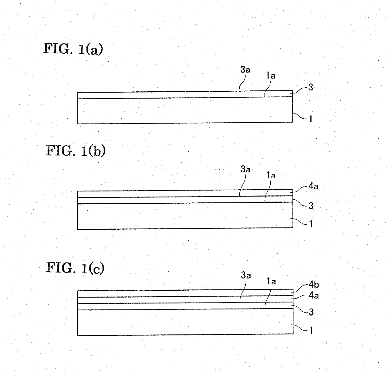
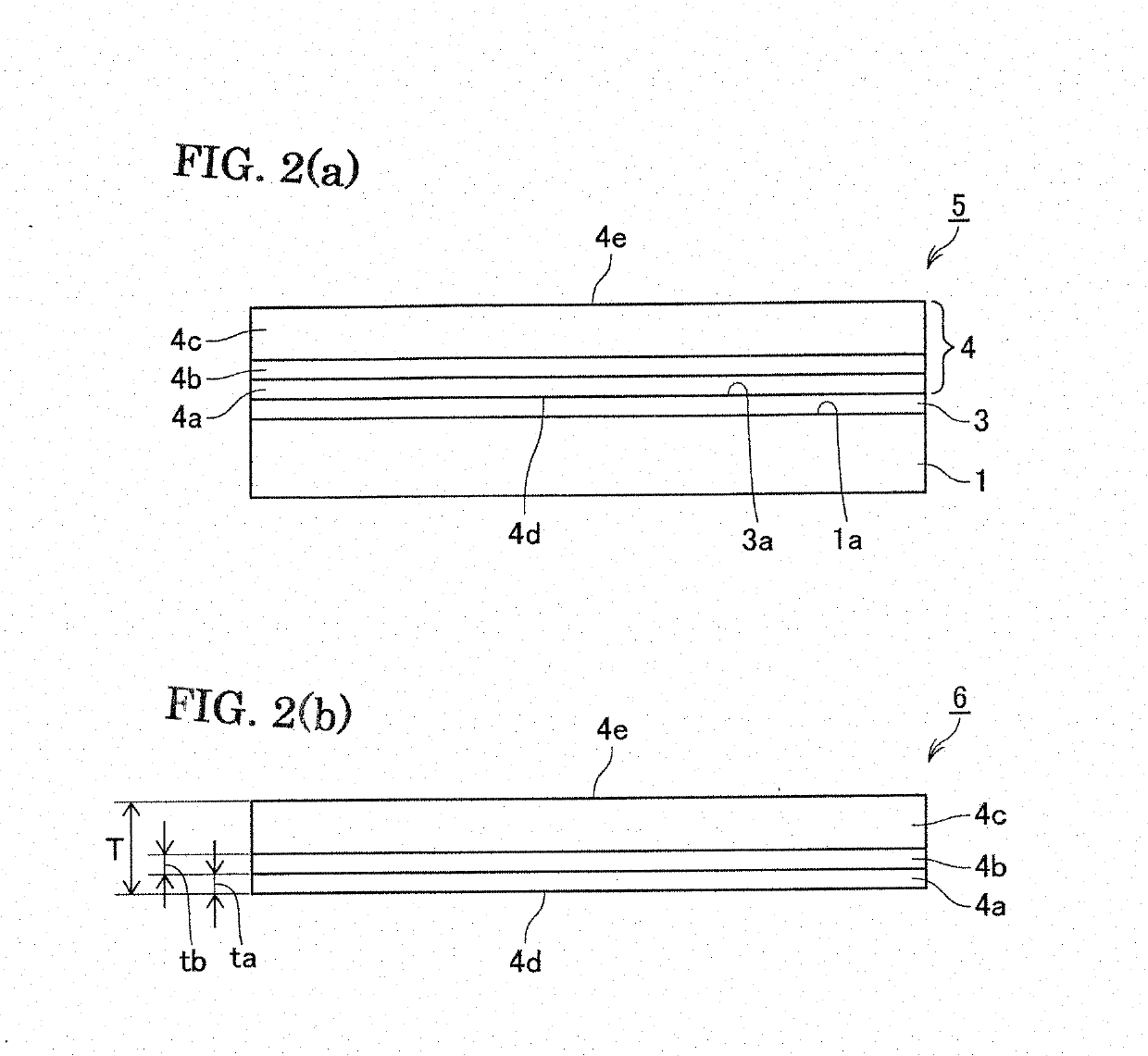
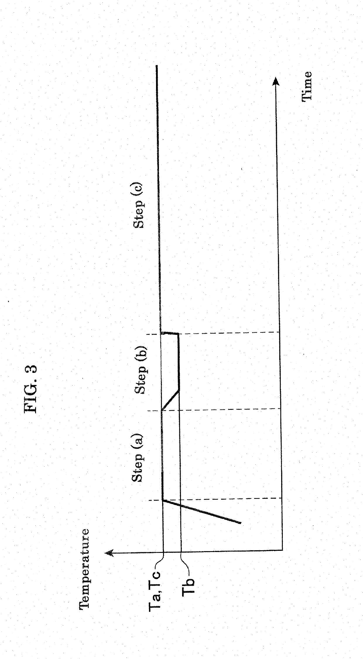
[0064]The gallium nitride crystal layer was grown according to the method described referring to FIGS. 1 to 3.
[0065]Specifically, it was epitaxially grown a seed crystal film 3 of gallium nitride having a thickness of 5 microns on a c-plane sapphire body having a diameter of 3 inches and thickness of 0.25 mm by MOCVD method to produce so-called GaN template (FIG. 1(a)).
[0066]The seed crystal layer 4 was then grown on the seed crystal film 3 by flux method.
[0067]Specifically, it was used a cylindrical crucible with a flat bottom with an inner diameter of 80 mm and a height of 45 mm, materials for growth (Ga metal 60 g and Na metal 60 g) were molten in a glove box and then filled into the crucible. Na was filled in advance and Ga was filled thereafter, so that Na was shielded from an atmosphere to prevent the oxidation of Na. The height of the melt of the materials in the crucible was about 15 mm.
[0068]The crucible was contained and sealed in a container of a heat-r...
##ventive examples 2 to 7
Inventive Examples 2 to 7
[0084]The nitride layers of the group 13 element according to the respective examples were film-formed.
[0085]However, the respective condition of the steps (a), (b) and (c) were changed as shown in table 1.
[0086]The structure of each layer of the thus obtained nitride layers of the group 13 element was shown in table 2. Further, in the thus obtained nitride layers of the group 13 element of the respective examples, the presence or absence of the cracks in each nitride layer of the group 13 element was observed after the growth and separation by laser lift-off method. The results were shown in table 2.
TABLE 1Step (a)Step (b)Step(c)Ro-Ro-Stop-Temp.rota-rota-stop-rota-rota-stop-tationtationpingDescendenttiontionpingtiontionpingTemp.TimeratetimetimerateTemp.timeratetimetimeTemp.timeratetimetime° C.hrsrpmsecsec° C. / hrs° C.hrsrpmsecsec° C.hrsrpmsecsecEx. 1870510600600308403106006008709210600600Ex. 28701010600600308403106006008708710600600Ex. 3870510600600128403106...
PUM
| Property | Measurement | Unit |
|---|---|---|
| thickness | aaaaa | aaaaa |
| length | aaaaa | aaaaa |
| grain size | aaaaa | aaaaa |
Abstract
Description
Claims
Application Information


