Touch panel device and method for manufacturing touch panel devices

Active Publication Date: 2006-02-23
FUJITSU LTD
View PDF3 Cites 20 Cited by
  • Summary
  • Abstract
  • Description
  • Claims
  • Application Information

AI Technical Summary

Benefits of technology

[0023] As necessary, the step for forming the piezoelectric thin film includes forming the piezoelectric thin film using zinc oxide and simultaneously forming a girdle wall using the zinc oxide between two of the plural wiring electrodes on the substrate so as to prevent migration when the wiring electrode is printed.
[0024] According to the present invention, a width of a bezel portion of the touch panel device can be reduced as much as possible, while increase of a thickness of the touch panel device

Problems solved by technology

It is not good to increase a thickness of the touch pane

Method used


Image

  • Touch panel device and method for manufacturing touch panel devices
  • Touch panel device and method for manufacturing touch panel devices
  • Touch panel device and method for manufacturing touch panel devices

Examples


Example

First Embodiment

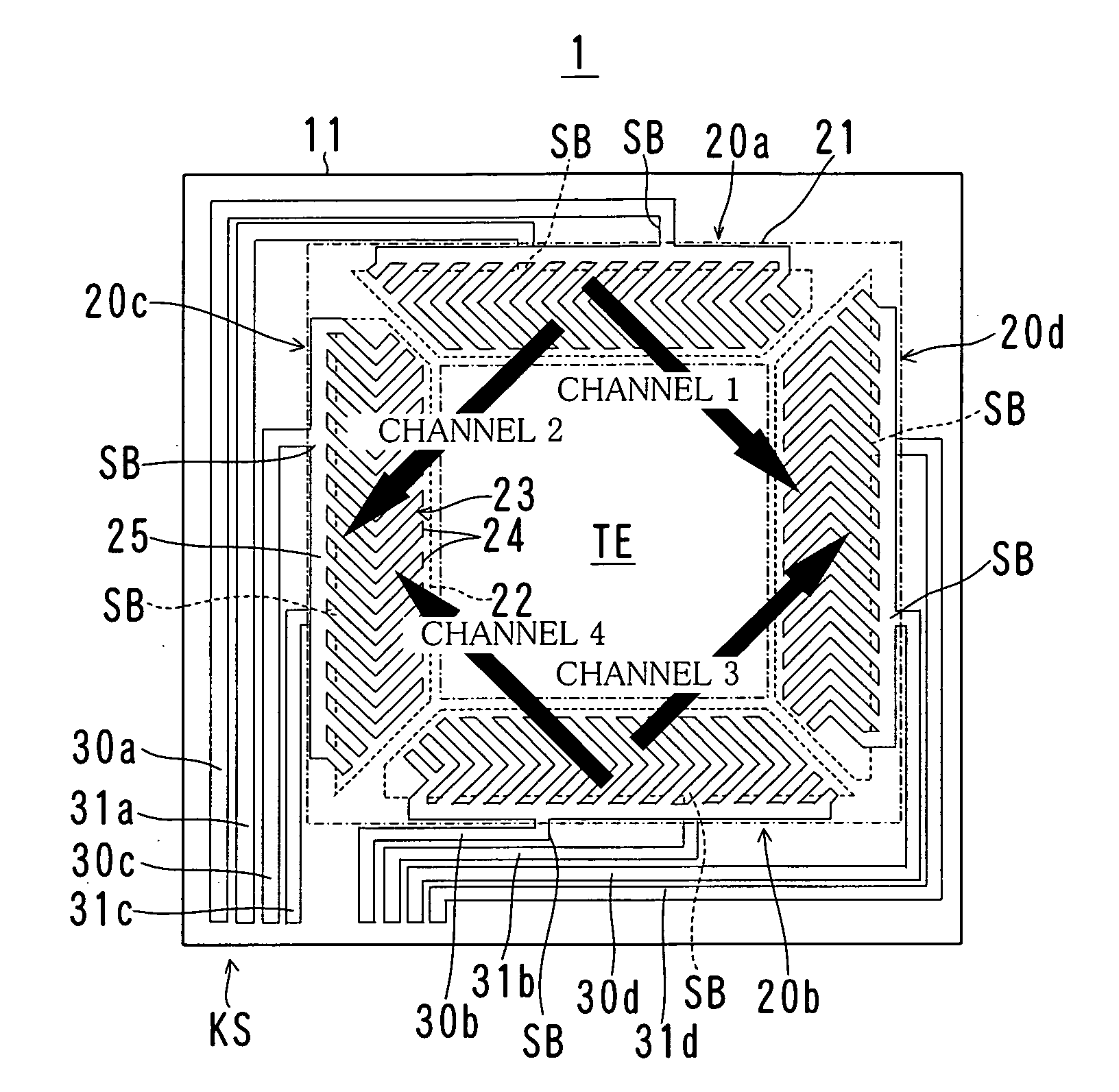
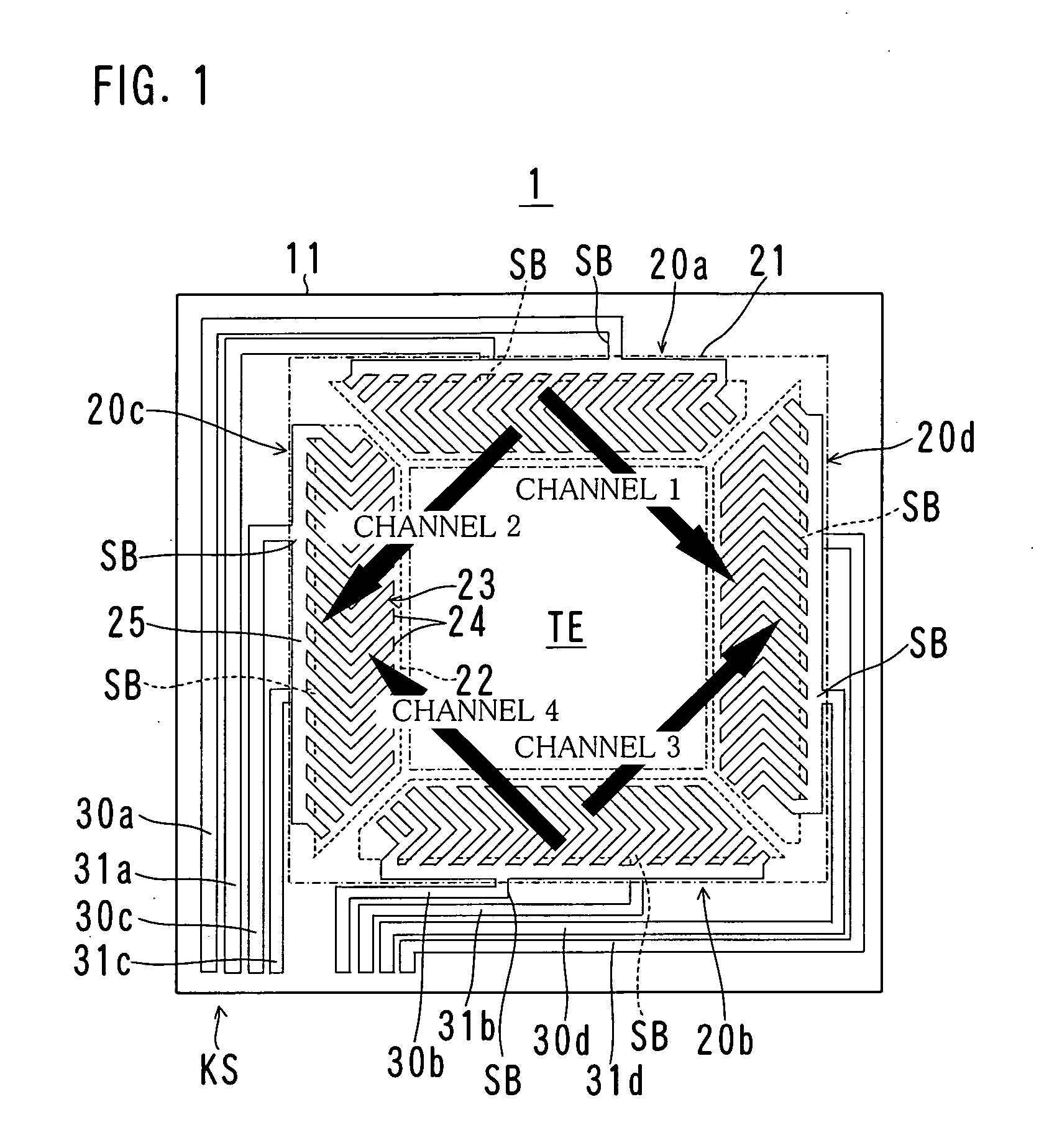
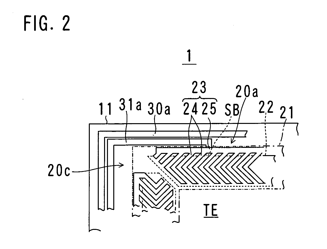
[0039]FIG. 1 is a plan view of a touch panel device 1 according to a first embodiment of the present invention, FIG. 2 is an enlarged view of a part of the touch panel device 1, FIG. 3 is a cross section of a portion of a transducer 20 and wiring electrodes 30 and 31 of the touch panel device 1 shown in an enlarged manner, FIG. 4 shows a position of a connection portion SB, FIG. 5 shows an example of a voltage distribution of the transducer 20, FIG. 6 shows waveforms of an excitation signal and a received signal, FIG. 7 is a diagram for explaining a general process for manufacturing the transducer 20, FIG. 8 is a cross section showing an example of providing an anchor 35 at a base portion of the wiring electrodes 30 and 31.

[0040] As shown in FIG. 1, the touch panel device 1 includes a rectangular transparent glass substrate 11, four transducers 20a-20d disposed at the periphery of the substrate 11, and wiring electrodes 30a-30d and 31a-31d disposed at the edge port...

Example

[0072] Here, only differences between the first and the second embodiments will be described.

[0073]FIG. 9 is a cross section of a portion of transducer 20B and wiring electrodes 30B and 31B of the touch panel device 1B according to a second embodiment of the present invention shown in an enlarged manner, and FIG. 10 is a plan view corresponding to FIG. 9.

[0074] As shown in FIGS. 9 and 10, the bus electrode 25B is formed not on the surface of the piezoelectric thin film 21B but on the surface of the glass substrate 11. Namely, the bus electrode 25B includes an electrode base portion 251 that is formed on the surface of the glass substrate 11 by printing nano silver paste and an electrode main body 252 that is formed on the electrode base portion 251 by printing hybrid nano silver paste. The electrode base portion 251 has a thickness of approximately 2-3 microns for example and a width of approximately 100-150 microns for example. The electrode main body 252 has a thickness of appro...

Example

[0078] Here, only differences between the first and the third embodiments will be described.

[0079]FIG. 11 is a cross section of a portion of the transducer 20C and wiring electrodes 30C and 31C of the touch panel device 1C according to the third embodiment of the present invention. FIG. 11 shows a cross section cut by a plane including a connection portion SB of a plate electrode 22C with a wiring electrode 31C.

[0080] As shown in FIG. 11, the plate electrode 22C, a piezoelectric thin film 21C and a comb-like electrode 23C are formed on the surface of the glass substrate 11. The plate electrode 22C is a thin film of aluminum having a thickness of approximately 0.3 microns for example and is provided so as to extend a little from and under the piezoelectric thin film 21C. The piezoelectric thin film 21C is a thin film of zinc oxide having a thickness of approximately 2 microns, for example. The comb-like electrode finger 24C is a thin film made of nano silver paste having a thicknes...


PUM


Abstract

Each of transducers of a touch panel device includes a piezoelectric thin film, a plate electrode disposed at one surface of the piezoelectric thin film and a comb-like electrode disposed at the other surface of the piezoelectric thin film. The comb-like electrode has a plurality of comb-like electrode fingers and a linear bus electrode to which one end of each of the plural comb-like electrode fingers is connected. A plurality of wiring electrodes is provided at the outer side of any of the transducers in parallel with the bus electrode of the transducer and is connected to the bus electrode and the plate electrode of any of the transducers. Each of the wiring electrodes includes an electrode base portion formed by printing silver paste containing fine particles on the substrate and an electrode main body formed by printing silver paste containing large particles and fine particles in a mixed manner on the electrode base portion.

Description

BACKGROUND OF THE INVENTION [0001] 1. Field of the Invention [0002] The present invention relates to a touch panel device that determines a touch position of an object by detecting attenuation position of a surface acoustic wave due to a touch of the object. The touch panel device is used as an input device of a personal computer or a personal digital assistant, for example. [0003] 2. Description of the Prior Art [0004] As an input device of a personal computer, a mobile computer, a personal digital assistant device (PDA) or the like, the touch panel device is often used in which information can be entered with the touch of a finger or a pen on a display screen of a display device. [0005] There are two types of the touch panel devices. One utilizes a resistance film, and another utilizes a surface acoustic wave (SAW). The resistance film type has a multilayered resistance film in a touch area, which scatters light so that transmittance is low. A touch panel device of the surface aco...

Claims


Application Information

Patent Timeline
IPC IPC(8): G09G5/00
CPCG06F3/0436G06F3/03
Inventor SANO, SATOSHIKATSUKI, TAKASHITAKAHASHI, YUJINAKAZAWA, FUMIHIKO
Owner FUJITSU LTD
Why Eureka
Try Eureka