Method and system for reducing pin count in an integrated circuit when interfacing to a memory

Inactive Publication Date: 2006-02-23
AVAGO TECH INT SALES PTE LTD
View PDF2 Cites 25 Cited by
  • Summary
  • Abstract
  • Description
  • Claims
  • Application Information

AI Technical Summary

Benefits of technology

[0019] According to the method and system disclosed herein, the present invention reduces the number of pins required to interface to an SDRAM from an IC while still adhering to the industry standard. In designs where memory speed is not an issue, the availability of extra pins reduces the cost of production, reduces the amount of power required, and reduces noise. In many systems the presence of high speed I/O signal switching creates noise that

Problems solved by technology

In many systems the presence of high speed I/O signal

Method used


Image

  • Method and system for reducing pin count in an integrated circuit when interfacing to a memory
  • Method and system for reducing pin count in an integrated circuit when interfacing to a memory
  • Method and system for reducing pin count in an integrated circuit when interfacing to a memory

Examples


Embodiment Construction

[0028] The present invention relates to integrated circuits, and more particularly to reducing pin count in an integrated circuit when interfacing to a memory. The following description is presented to enable one of ordinary skill in the art to make and use the invention and is provided in the context of a patent application and its requirements. Various modifications to the preferred embodiments and the generic principles and features described herein will be readily apparent to those skilled in the art. Thus, the present invention is not intended to be limited to the embodiments shown, but is to be accorded the widest scope consistent with the principles and features described herein.

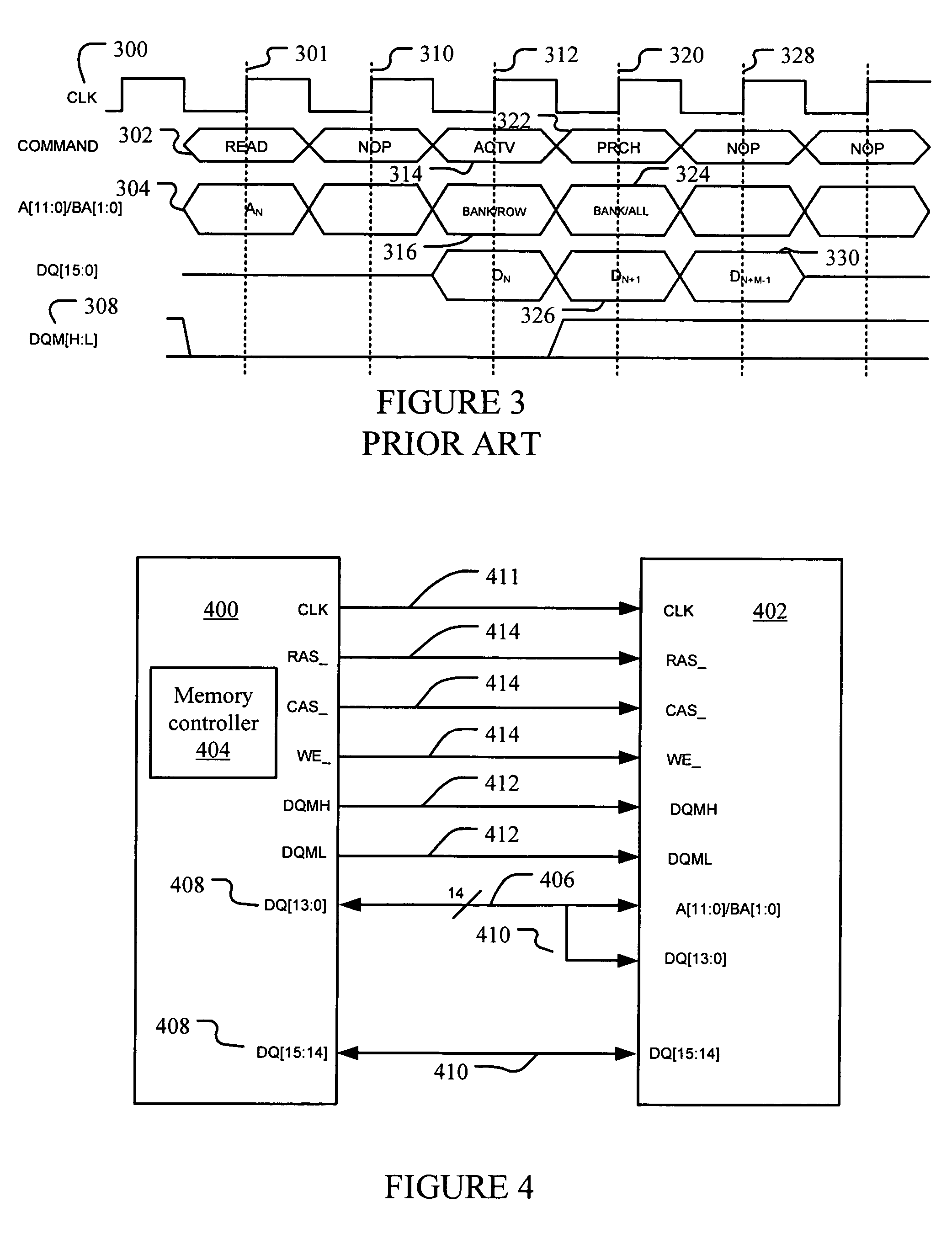
[0029]FIG. 4 is a block diagram illustrating one embodiment of the invention with integrated circuit (IC) 400 connected to synchronous dynamic random access memory (SDRAM) 402. IC 400 may be an application specific integrated circuit (ASIC) while SDRAM 402 may be an industry standard 64 or 128-Mbit s...


PUM


Abstract

The invention provides a system and method for reducing pin count in an integrated circuit (IC) when interfacing to a synchronous dynamic random access memory (SDRAM). The SDRAM has a plurality of address lines and a plurality of data lines. The method includes connecting together the plurality of data lines and the plurality of address lines. The IC interfaces to the SDRAM through the connected plurality of address lines and the plurality of data lines.

Description

FIELD OF THE INVENTION [0001] The present invention relates to integrated circuits, and more particularly to reducing pin count in an integrated circuit when interfacing to a memory. BACKGROUND OF THE INVENTION [0002] The majority of designs in the consumer electronic industry include an interface between an integrated circuit (IC) and a memory, the memory often known as a synchronous dynamic random access memory (SDRAM). An SDRAM is a memory chip, with different SDRAMs designed to hold different amounts of data and operate at different speeds. [0003] De facto industry standards exist for the interface between an IC and a SDRAM. To better understand the limitations and operation of conventional systems, an example of an IC interfaced to a SDRAM according to the de facto standard is provided, along with write and read operations. [0004]FIG. 1 is a block diagram illustrating a conventional IC 100 connected to standard SDRAM 102. IC 100 has memory controller 104 that operates SDRAM 102...

Claims


Application Information

Patent Timeline
IPC IPC(8): G06F12/00
CPCG11C5/066G06F13/4243
Inventor CHARLES, GORDONWASHINGTON, EMANUEL
Owner AVAGO TECH INT SALES PTE LTD
Why Eureka
Try Eureka