

Multilayer circuit board and method of producing the same
- Summary
- Abstract
- Description
- Claims
- Application Information
AI Technical Summary
Benefits of technology
Problems solved by technology
Method used
Image

Examples
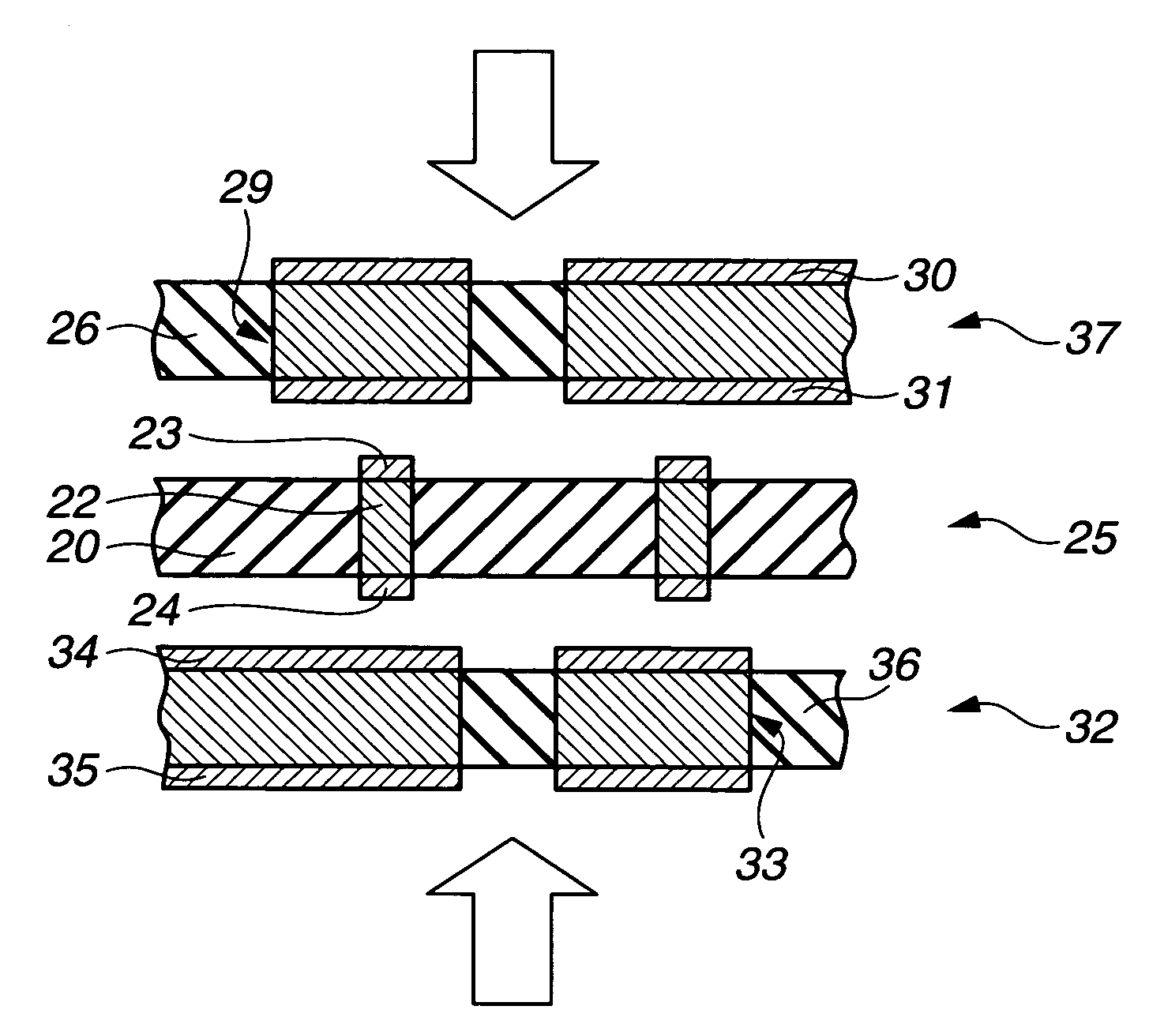
example 1
(Production of Via-Forming Sheet)
[0050] A photosensitive resin composition was coated on a stainless steel support 19 having a thickness of 100μ, and dried at 80° C. for 30 minutes to provide a coating film 20 having a thickness of 50μ, as shown in FIG. 5a. The coating film 20 was contacted with a negative mask, and irradiated with an extra-high pressure mercury lamp at 1000 mj / cm2. Unexposed portions were developed by using an organic solvent at a spray pressure of 2 Kg / cm2 for 1 minute.
[0051] The support 19 coated with the coating film 20 was heated and cured at 160° C. for 1 hour to form vias 21 each having a depth of 50μ, as shown in FIG. 5b. The vias 21 were electroplated with copper 22 to a thickness of about 50μ, whereby the vias 21 were completely filled with the copper 22, as shown in FIG. 5c. The surfaces of the copper 22 on the support 19 was polished by a ceramic buff at a load power of 1.5 ampere, as shown in FIG. 5d. After the polishing, the support 19 was peeled aw...
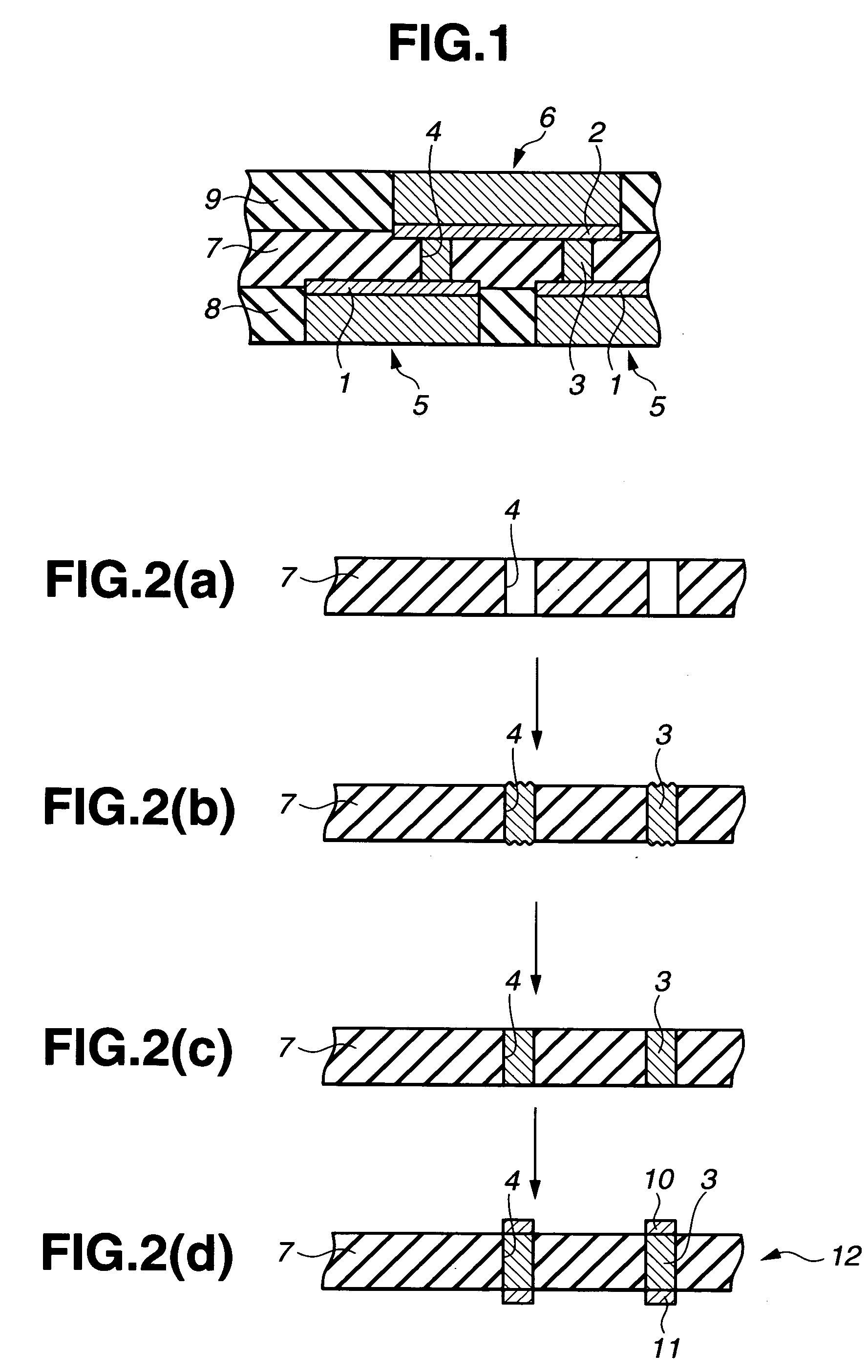
example 2
(Production of Via-Forming Sheet)
[0057] A thermosetting resin composition was coated on a stainless steel support 19 having a thickness of 100μ, and dried at 160° C. for 60 minutes to provide a coating film 40 having a thickness of 50μ, as shown in FIG. 9a. Vias 41 each having a depth of 50μ were formed in the coating film 40 using a carbon dioxide gas laser, as shown in FIG. 9b. The vias 41 were electroplated with copper 42 to a thickness of about 50μ, whereby the vias 41 were completely filled with the copper 42, as shown in FIG. 9c. The surfaces of the copper 42 on the support 19 were polished by a ceramic buff at a load power of 1.5 ampere, as shown in FIG. 9d. After the polishing, the support 19 was peeled away, as shown in FIG. 9e. The surfaces of the vias 41 filled with the copper 42 was subjected to tin electroless plating to form plated layers 43 and 44, each having a thickness of 1μ, on the surface of the via 41, as shown in FIG. 9f. Thus, a via sheet 45, i.e., a via-for...
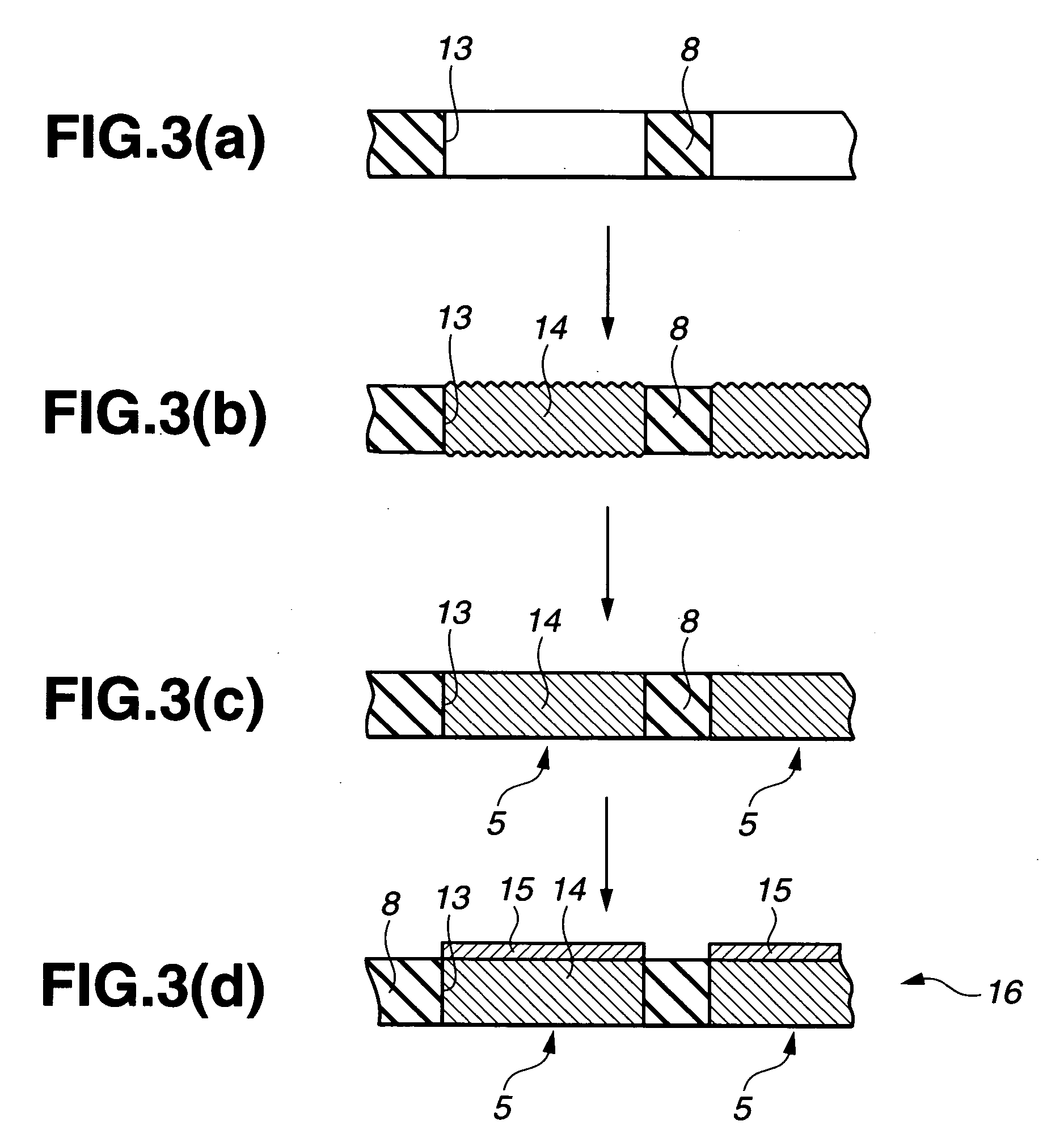
example 3
(Production of Via-Forming Sheet)
[0062] Similar to Example 1, a thermosetting type PPE film was coated on the stainless steel support, and heated and cured by a vacuum press machine at 200° C. for 2 hours. The vias were formed, and polished. The support was peeled away. The electroless tin—silver plating was subjected to form a plated layer having a thickness of 1μ. Thus, a via sheet was produced.
(Production of Circuit Pattern-Forming Sheet)
[0063] Similar to Example 1, two pattern sheets each having a thickness of 30μ were produced.
(Production of Multilayer Circuit Board)
[0064] Similar to Example 1, the via sheet was sandwiched between two pattern sheets, and was heated and pressed by a vacuum press machine at 220° C. for 120 minutes. Thus, a multilayer circuit board (double-sided printed wiring board) according to the present invention was produced.
[0065] According to the present invention, the vias and the conductor wiring layer are joined with an alloy in the multilayer ...
PUM
 Abstract
Description
Claims
Application Information