Packaged microelectronic imaging devices and methods of packaging microelectronic imaging devices

a microelectronic imaging and packaging technology, applied in the direction of basic electric elements, semiconductor devices, electrical equipment, etc., can solve the problems of occupying a significant amount of vertical space, limiting the design and marketability of conventional packaged microelectronic imagers, and occupying a large footprin

Active Publication Date: 2006-03-02
APTINA IMAGING CORP
View PDF93 Cites 91 Cited by
  • Summary
  • Abstract
  • Description
  • Claims
  • Application Information

AI Technical Summary

Problems solved by technology

One problem with conventional packaged microelectronic imagers is that they have relatively large footprints and occupy a significant amount of vertical space (i.e., high profiles).
Accordingly, the footprint of conventional packaged microelectronic imagers can be a limiting factor in the design and marketability of picture cell phones or PDAs because these devices are continually shrinking to be more portable.
Another problem with con

Method used


Image

  • Packaged microelectronic imaging devices and methods of packaging microelectronic imaging devices
  • Packaged microelectronic imaging devices and methods of packaging microelectronic imaging devices
  • Packaged microelectronic imaging devices and methods of packaging microelectronic imaging devices

Examples


Embodiment Construction

A. Overview

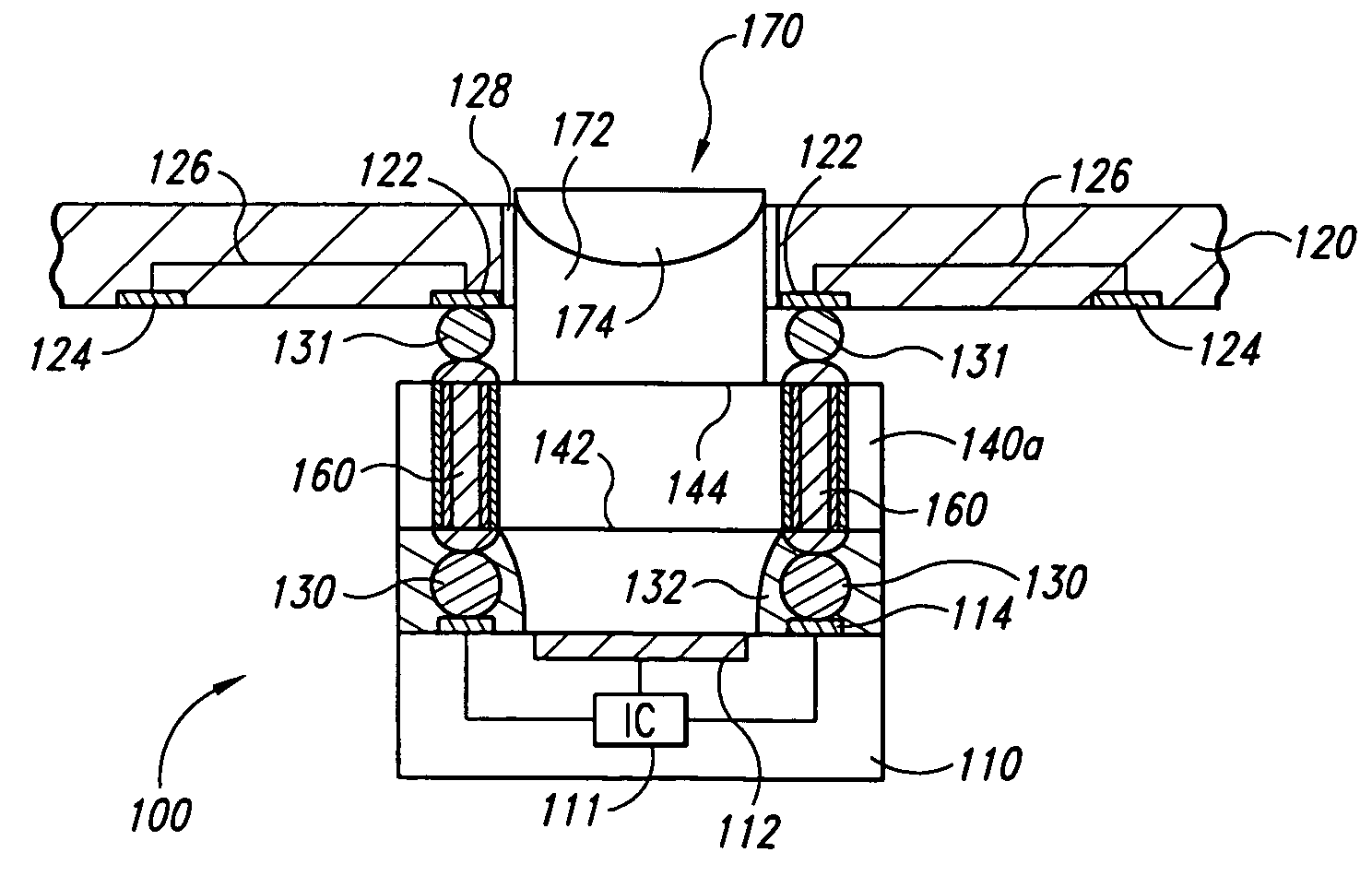
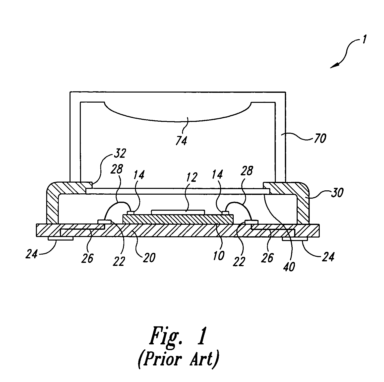
[0025] The following disclosure describes several embodiments of microelectronic imaging devices and methods of packaging microelectronic imaging devices. Specific details of several embodiments of the invention are described below with reference to CMOS imagers to provide a thorough understanding of these embodiments, but other embodiments can be CCD imagers or other types of imaging devices. Several details describing well-known structures often associated with microelectronic devices are not set forth in the following description to avoid unnecessarily obscuring the description of the disclosed embodiments. Additionally, several other embodiments of the invention can have different configurations and / or components than those described in this section. As such, a person of ordinary skill in the art will accordingly understand that the invention may have other embodiments with additional elements or without several of the elements shown and described below with reference...


PUM


Abstract

Microelectronic imaging devices and methods of packaging microelectronic imaging devices are disclosed herein. In one embodiment, a microelectronic imaging device includes a microelectronic die having an integrated circuit, an image sensor electrically coupled to the integrated circuit, and a plurality of bond-pads electrically coupled to the integrated circuit. The imaging device further includes a cover over the image sensor and a plurality of interconnects in and/or on the cover that are electrically coupled to corresponding bond-pads of the die. The interconnects provide external electrical contacts for the bond-pads of the die. The interconnects can extend through the cover or along a surface of the cover.

Description

TECHNICAL FIELD [0001] The present invention is related to microelectronic devices and methods for packaging microelectronic devices. Several aspects of the present invention are directed toward packaging microelectronic imaging devices that are responsive to radiation in the visible light spectrum or radiation in other spectrums. BACKGROUND [0002] Microelectronic imagers are used in digital cameras, wireless devices with picture capabilities, and many other applications. Cell phones and Personal Digital Assistants (PDAs), for example, incorporate microelectronic imagers for capturing and sending digital images. The use of microelectronic imagers in electronic devices has been steadily increasing as imagers become smaller and produce higher quality images with increased pixel counts. [0003] Microelectronic imagers include image sensors that use Charged Coupled Device (CCD) systems, Complementary Metal-Oxide Semiconductor (CMOS) systems, or other systems. CCD image sensors have been ...

Claims


Application Information

Patent Timeline
IPC IPC(8): H01L21/00H01L27/14H01L31/0232
CPCH01L24/94H01L2924/01074H01L27/14625H01L27/14634H01L27/1469H01L31/0203H01L2224/48091H01L2224/48227H01L2924/01029H01L2924/01077H01L2924/01078H01L27/14618H01L2924/01033H01L2924/01005H01L2924/01006H01L2924/00014H01L2924/14H01L2924/00
Inventor WATKINS, CHARLES M.HEMBREE, DAVID R.BENSON, PETER A.AKRAM, SALMAN
Owner APTINA IMAGING CORP
Why Eureka
Try Eureka