Unlock instant, AI-driven research and patent intelligence for your innovation.

Semiconductor memory device

a memory device and semiconductor technology, applied in the field of semiconductor memory devices, can solve the problems of becoming difficult to provide flash memory with high-speed data read performance under the condition of a more lowered voltage, becoming difficult to do timing control of read data output operation, and becoming impossible to secure the time period necessary for setting up data

Inactive Publication Date: 2006-03-02
KK TOSHIBA
View PDF9 Cites 22 Cited by
  • Summary
  • Abstract
  • Description
  • Claims
  • Application Information

AI Technical Summary

Benefits of technology

[0013] a control signal generation circuit configured to generate a plurality of control signals based on a reference clock signal externally supplied, the control signals serving for controlling data input and output of the sense amplifier circuit and data transferring timing in the data transfer circuit; and
[0014] an internal cloc

Problems solved by technology

However, in such a scheme that read data output operation is directly controlled by the read enable signal supplied from the external, it becomes difficult to provide a flash memory with a high-speed data read performance under the condition of a more lowered voltage.
In case the read enable signal supplied to the flash memory is declined in change rate, and duty ratio thereof is changed due to noises on the external bus line, load variations of the bus line, impedance mismatching between the driver of an external controller and load thereof including the bus line, and the like, it becomes difficult to do timing control of the read data output operation.
In detail, it may become impossible to secure a time period necessary for setting up data on the data output path disposed between the sense amplifier circuit and the input / output ports.
This causes the flash memory to read erroneous data and / or data with erroneous addresses.

Method used


Image

  • Semiconductor memory device
  • Semiconductor memory device
  • Semiconductor memory device

Examples


embodiment 1

[0038] [Embodiment 1]

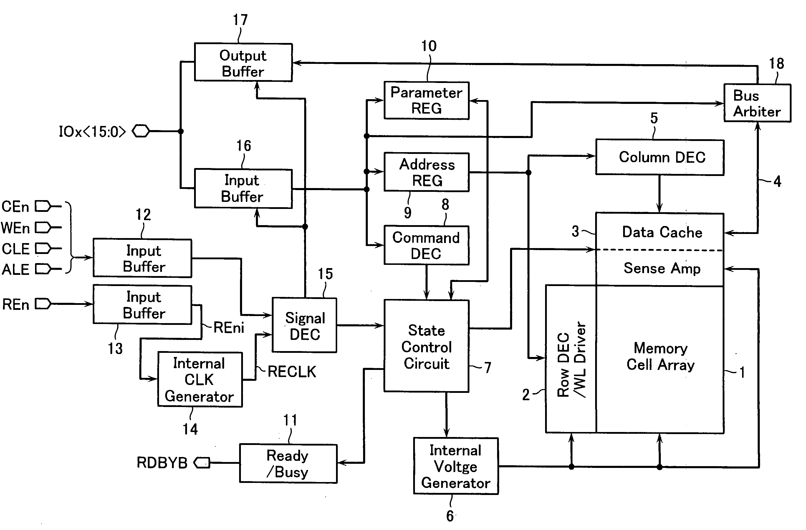
[0039]FIG. 1 shows a functional block diagram of a NAND-type flash memory in accordance with an embodiment. The memory cell array 1 is, as shown in FIGS. 2 and 3, formed of NAND cell units NU arranged in a matrix manner. Each NAND cell unit NU has a plurality of electrically rewritable and non-volatile memory cells (i.e., thirty two cells in the example shown in FIG. 3) M0-M31 connected in series and select gate transistors S1 and S2, which serve for coupling the both ends of the serially connected memory cells to a bit line BL and a common source line CELSRC, respectively.

[0040] A set of NAND cell units sharing a word line constitutes a block, which serves as a unit of data erase. As shown in FIG. 2, plural blocks (BLK0, BLK1, . . . ) are arranged in the direction of the bit line.

[0041] As shown in FIG. 3, each two bit lines BLa and BLb share a sense amplifier PB. The bit lines BLa and BLb are selectively coupled to the sense amplifier PB via bit line select ...

embodiment 2

[0086] [Embodiment 2]

[0087]FIG. 14 shows a functional block diagram of a NAND-type flash memory in accordance with Embodiment 2. The portions corresponding to those in FIG. 1 are denoted by the same reference signs as in FIG. 1, and detailed explanation thereof will be omitted.

[0088] In this Embodiment 2, the parameter register 10, which is usually utilized only in a test mode, is configured to be able to store a control parameter, which is used for adapting the chip to operation circumstances (for example, read configuration), and output it for setting and / or changing operation circumstances corresponding to a host device in response to a specified circumstance setting command.

[0089]FIG. 15 shows input / output relationships of the parameter register 10 in accordance with this embodiment. In case of setting data DIN7:0> in the parameter register 10 together with a test mode signal TESTMODE, the parameter register 10 outputs test-use parameter TESTPAR7:0>. In addition, in this embod...

embodiment 3

[0102] [Embodiment 3]

[0103]FIG. 19 shows a NAND-type flash memory in accordance with another embodiment where not only a data read operation but also a data write operation are taken in for improving operation speed thereof. A detailed explanation will be omitted because the main portions corresponding to those in FIG. 14 are denoted by the same reference signs as in FIG. 14.

[0104] An internal clock generation circuit 14a is disposed at the output node of the input buffer 13a disposed in association with the read enable signal REn. This is the same as above-described Embodiments 1 and 2. In this Embodiment 3, another internal clock generation circuit 14b is disposed at the output node of another input buffer 13b disposed in association with the write enable signal WEn. These internal clock generation circuits 14a and 14b may be formed as similar to that described in Embodiment 1.

[0105] In a data write mode, write command and write address are input as synchronous with the write en...


PUM


Abstract

A semiconductor memory device includes: a memory cell array, in which electrically rewritable and non-volatile memory cells are arranged; a sense amplifier circuit configured to be coupled to the memory cell array; a data transfer circuit disposed between the sense amplifier circuit and data input / output ports; a control signal generation circuit configured to generate a plurality of control signals based on a reference clock signal externally supplied, the control signals serving for controlling data input and output of the sense amplifier circuit and data transferring timing in the data transfer circuit; and an internal clock signal generation circuit configured to generate an internal clock signal based on the reference clock signal for serving as the basis of the control signals, the internal clock signal having the same clock cycle as the reference clock signal and a constant duty ratio without regard to the duty ratio of the reference clock signal.

Description

CROSS-REFERENCE TO RELATED APPLICATION [0001] This application is based on and claims the benefit of priority from the prior Japanese Patent Application No. 2004-244936, filed on Aug. 25, 2004, the entire contents of which are incorporated herein by reference. BACKGROUND OF THE INVENTION [0002] 1. Field of the Invention [0003] This invention relates to a semiconductor memory device having electrically rewritable and non-volatile memory cells. [0004] 2. Description of the Related Art [0005] A NAND-type flash memory is known as one of electrically rewritable and non-volatile semiconductor memories (EEPROMs). Since this flash memory is formed of NAND cell units, each of which has plural memory cells connected in series in such a manner that adjacent two memory cells share a source / drain diffusion layer, it is possible to lessen a unit cell area of a memory cell array, thereby providing a memory with a large capacitance. [0006] On the other hand, a NAND-type flash memory has a sense amp...

Claims


Application Information

Patent Timeline
IPC IPC(8): G11C16/06
CPCG11C16/0483G11C16/32G11C16/26G11C16/10
Inventor TOKIWA, NAOYA
Owner KK TOSHIBA