Optoelectronic arrangement having a surface-mountable semiconductor module and a cooling element

Active Publication Date: 2006-03-02
II VI DELAWARE INC
View PDF5 Cites 11 Cited by
  • Summary
  • Abstract
  • Description
  • Claims
  • Application Information

AI Technical Summary

Benefits of technology

[0023] Plastic housings for SMD devices that are filled with optically nontransparent potting compositions (also referred to as “black-molded”) achieve significantly higher temperature ranges than housings potted with a transparent material. Optically transparent potting comp

Problems solved by technology

Since the transmitting and/or receiving unit is intended to be connected to a further optical element in at least one light radiating direction, the SMD device is intended to be mounted by the mounting side

Method used


Image

  • Optoelectronic arrangement having a surface-mountable semiconductor module and a cooling element
  • Optoelectronic arrangement having a surface-mountable semiconductor module and a cooling element
  • Optoelectronic arrangement having a surface-mountable semiconductor module and a cooling element

Examples


Embodiment Construction

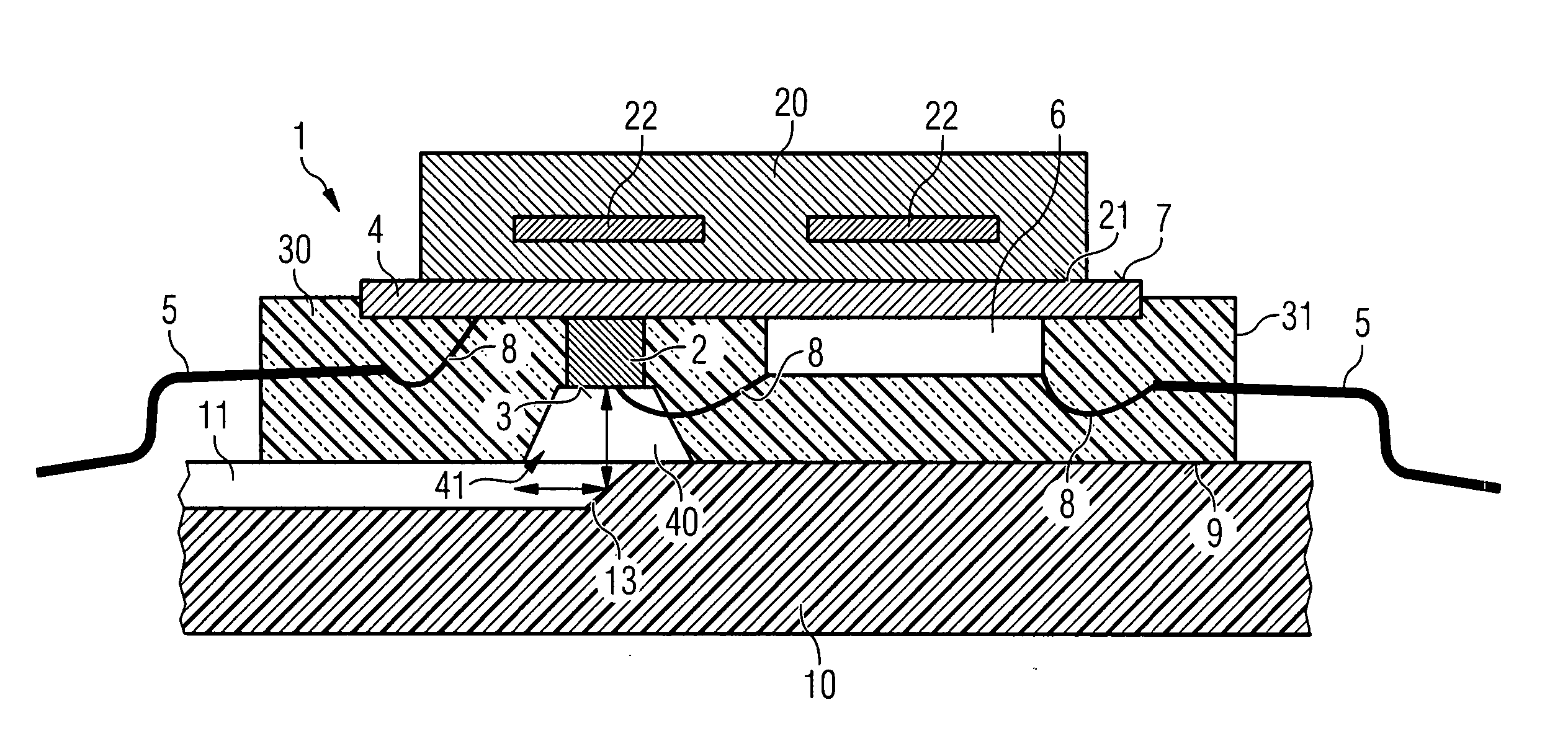
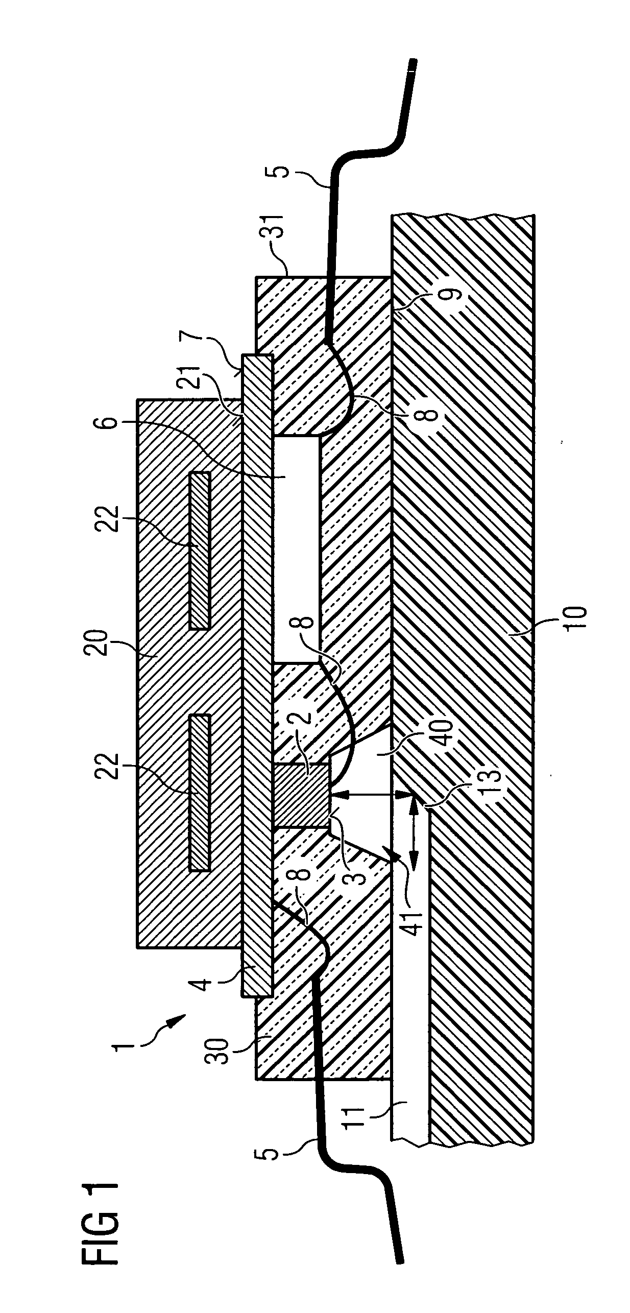
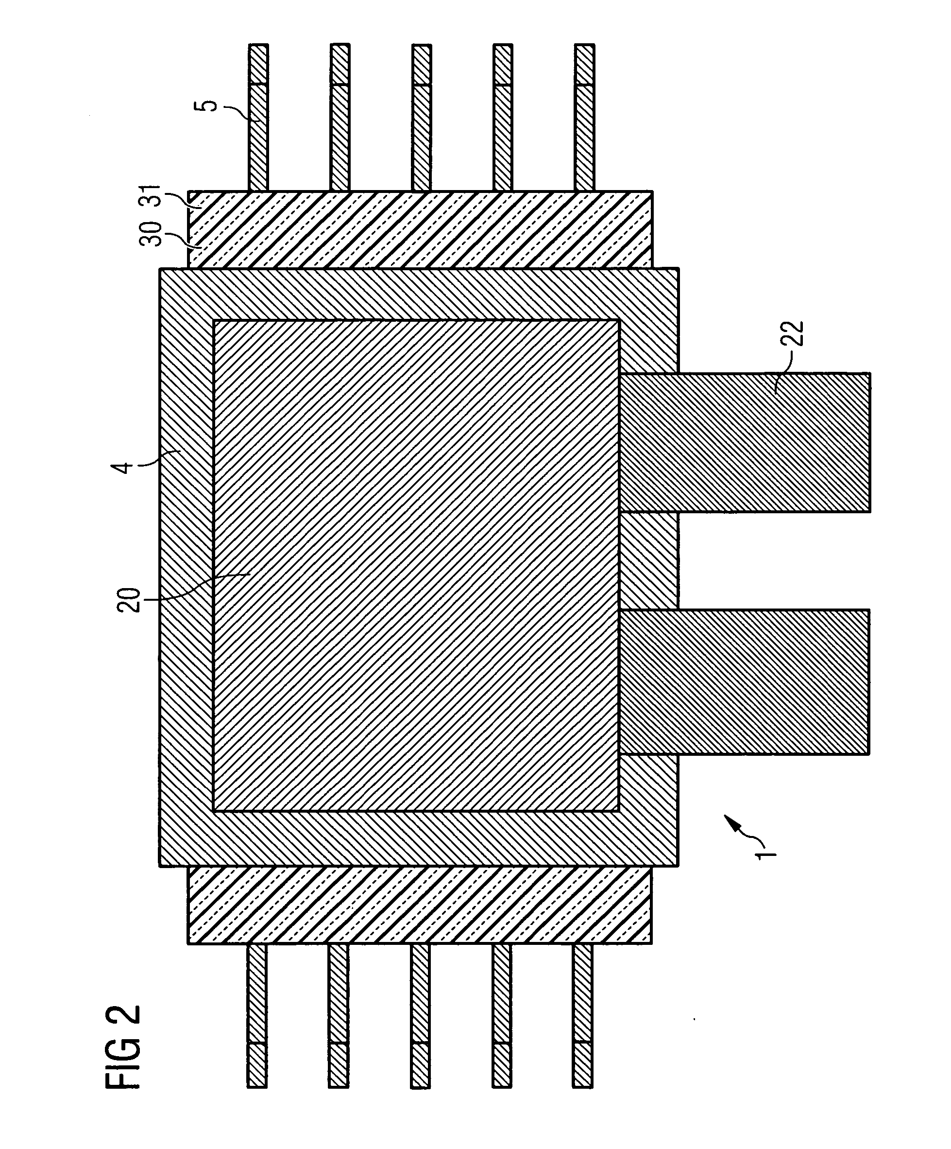
[0029]FIG. 1 shows a diagrammatic section through a surface-mountable semiconductor module 1, which is mounted on a printed circuit board 10 by means of contact legs 5 in such a way that its mounting side 9 points toward the printed circuit board 10.

[0030] In this case, the semiconductor module 1 first comprises a leadframe 4 arranged parallel to the printed circuit board 10. The contact legs 5, which arrange the leadframe in its position parallel to the printed circuit board 10, run between the leadframe 4 and the printed circuit board 10 and provide an electrical contact. Furthermore, the semiconductor module 1 comprises an optoelectronic transmitting and / or receiving unit 2. This may be for example a VCSEL, an LED or some other surface-mountable transceiver.

[0031] The printed circuit board 10 is composed of customary printed circuit board material or of a patterned plastic film (e.g. of Kapton®).

[0032] The optoelectronic transmitting and / or receiving unit (optoelectronic unit)...


PUM


Abstract

An optoelectronic arrangement having a surface-mountable semiconductor module having at least one optoelectronic transmitting and/or receiving unit, a housing, in which the optoelectronic transmitting and/or receiving unit is arranged, and a mounting side of the housing, which, in the case of surface mounting of the semiconductor module on a printed circuit board, faces the printed circuit board. The arrangement furthermore has a cooling element, which is thermally coupled to the semiconductor module for the purpose of cooling the optoelectronic transmitting and/or receiving unit. The cooling element is arranged on a side of the housing that is remote from the mounting side.

Description

RELATED APPLICATION [0001] The present application claims priority of U.S. patent application Ser. No. 60 / 606,279 filed by Martin Weigert on Aug. 31, 2004.FIELD OF THE INVENTION [0002] The invention relates to an optoelectronic arrangement having a surface-mountable semiconductor module and a cooling element. BACKGROUND OF THE INVENTION [0003] Surface-mountable semiconductor modules are also called SMD devices (“surface mounted devices”) and are usually arranged in a housing made of plastic. The arrangement comprising semiconductor component and housing is mounted by a mounting side of the housing on surfaces such as e.g. a side of a printed circuit board. [0004] Such a semiconductor module may have an optoelectronic transmitting and / or receiving unit via which light signals can be received and / or transmitted. Since the wavelength of the light signals is dependent on the temperature of the transmitting and / or receiving unit, it is known to provide a cooler for temperature stabilizat...

Claims


Application Information

Patent Timeline
IPC IPC(8): G02B6/26G02B6/42G02B6/12
CPCG02B6/4214G02B6/4201G02B6/4268G02B6/428
Inventor WEIGERT, MARTIN
Owner II VI DELAWARE INC
Why Eureka
Try Eureka