Electrical connector design and contact geometry and method of use thereof and methods of fabrication thereof

a technology of electrical connectors and contact surfaces, applied in the direction of coupling device details, coupling device connections, instruments, etc., can solve the problems of excessive force that must be applied to the electronic structure of the tip, the surface of the electrical contact locations on the contact surface may be too large to avoid damage to the electronic structure, etc., to achieve the effect of improving the electrical interconnection structure, high durability and reliability, and not easy to oxidiz

Inactive Publication Date: 2006-03-02
IBM CORP
View PDF30 Cites 29 Cited by
  • Summary
  • Abstract
  • Description
  • Claims
  • Application Information

AI Technical Summary

Benefits of technology

[0018] Yet another property of the present invention is to provide a probe construction that has high durability and reliability for repeated thermal and mechanical cycling. A further additional property of the present invention is to provide a probe structure that can be used for single chip or multiple chip wafer testing. Another property of the present invention is to provide a probe structure that has a hardened, pointed contact tip for penetrating the oxide films on the bond pads of IC devices.
[0019] The invention provides an improved electrical interconnection structure; test structure and test apparatus that utilizes compliant test elongated electrical conductor to make and maintain contact with electrical contact locations, e.g. bond, on the device to which electrical connection is made or being tested even if the bond pads are not all the same height. The invention provides a hardened point on the contact tip that is preferably made of a material that cannot be easily oxidized, and that has sufficient hardness to break through any oxidation that has accumulated on the bond pads. The invention preferably vibrates the tips to allow the hardened contact points to move back and forth across the electrical contact location, thereby further promoting the ability of the hardened contact points to break through any oxidation on the surface material such as electrical contact locality. Further, the invention provides slotted alignment sheets that maintain the compliant elongated electrical conductor in the proper position to remain in contact with the electrical contact locations even as the compliant elongated electrical conductors are being vibrated and pressed against the bond pads. Thus, the improved structure described above provides a number of significant advantages by providing test probes and electrical connectors that are compliant and can vibrate to break through any surface oxide on the contact location yet are positionally stable so as to remain in contact with the contact location. This allows many contact locations on one or more devices to be electrically contacted or tested with a single test device or connector structure which prevents individual elongated electrical conductors from disconnecting from their associated electrical contact locators and promotes many efficiencies with respect to electrically connecting to and testing integrated circuit devices.

Problems solved by technology

When there are a large number of flexible elongated electrical conductors the total force that must be applied to the electronic structure for the tip structures to sufficiently penetrate the surface of the electrical contact locations on the contact surface may be too large to avoid damage to the electronic structure.

Method used


Image

  • Electrical connector design and contact geometry and method of use thereof and methods of fabrication thereof
  • Electrical connector design and contact geometry and method of use thereof and methods of fabrication thereof
  • Electrical connector design and contact geometry and method of use thereof and methods of fabrication thereof

Examples


Embodiment Construction

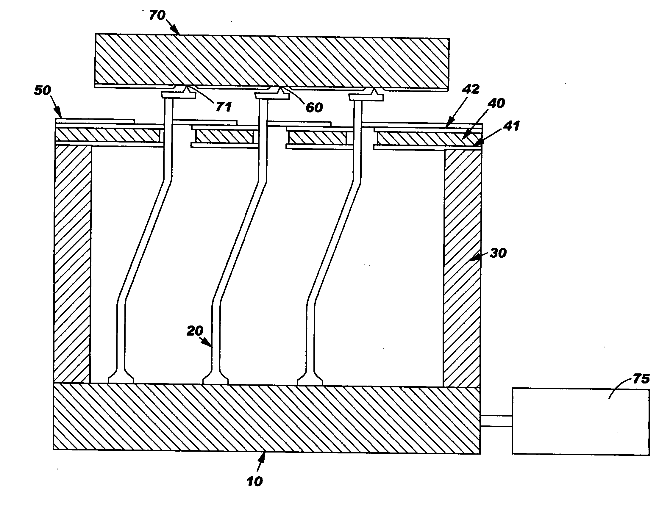
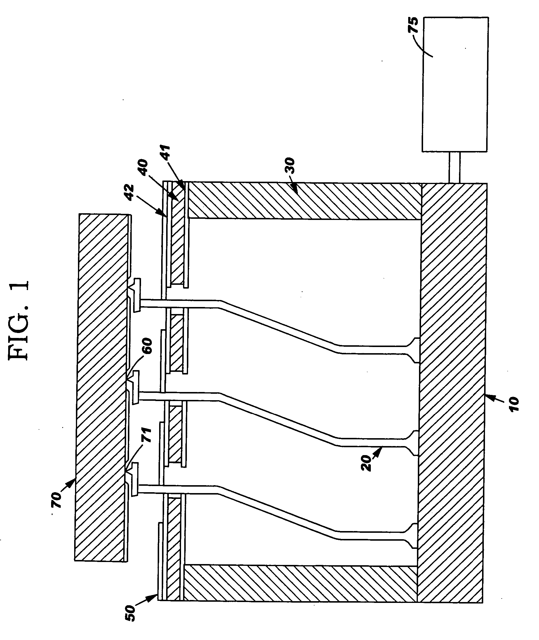
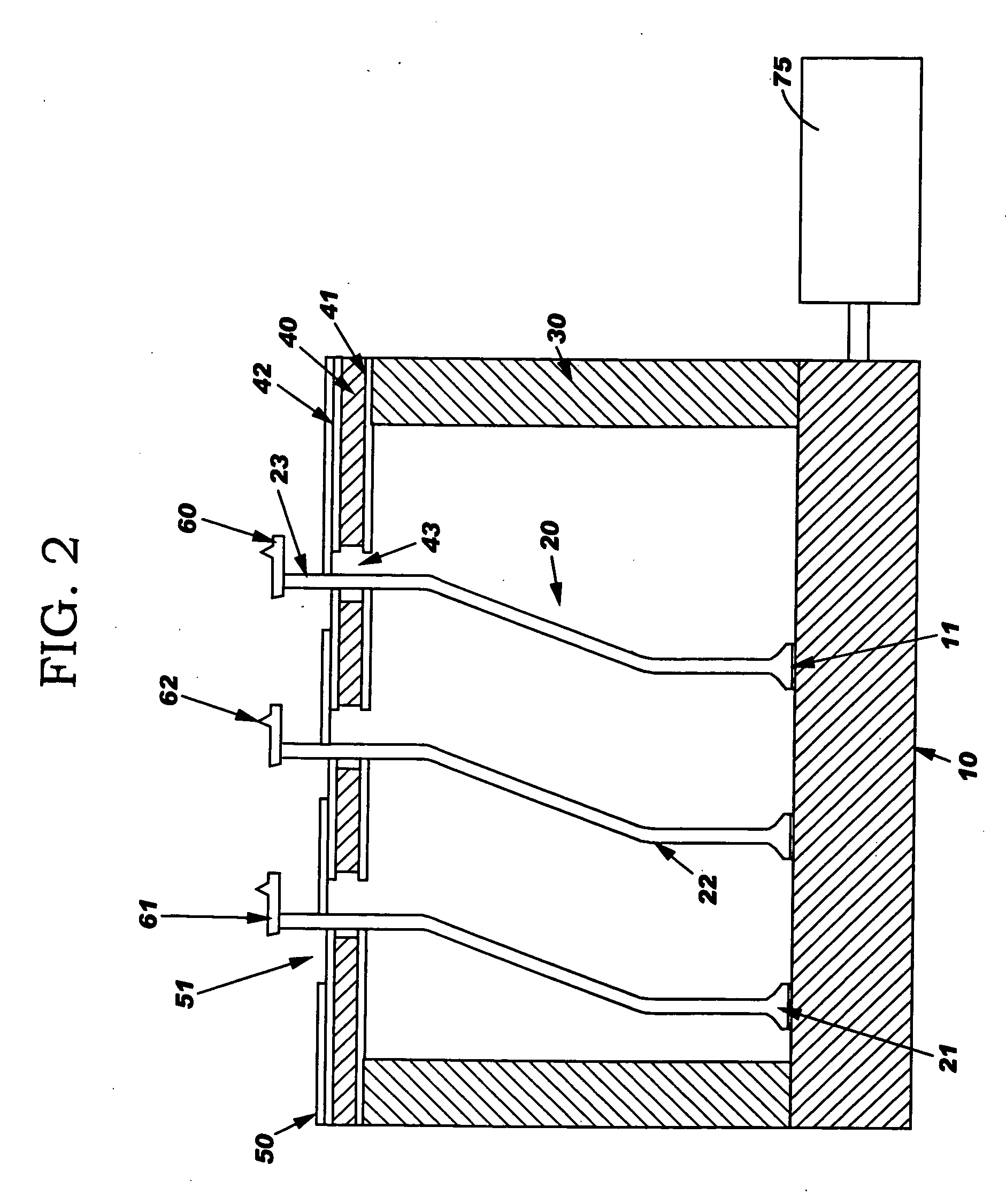
[0028] The present invention and the various features and advantageous details thereof are explained more fully with reference to the nonlimiting embodiments that are illustrated in the accompanying drawings and detailed in the following description. It should be noted that the features illustrated in the drawings are not necessarily drawn to scale. Descriptions of well-known components and processing techniques are omitted so as to not unnecessarily obscure the present invention. The examples used herein are intended merely to facilitate an understanding of ways in which the invention may be practiced and to further enable those of skill in the art to practice the invention. Accordingly, the examples should not be construed as limiting the scope of the invention.

[0029] While many examples discussed below relate to test probes used with a testing device, one ordinarily skilled in the art would readily understand that this is only one example in which the invention finds application...


PUM


Abstract

A probe or an electrical connector comprises a substrate with a surface having a plurality of electrical contact locations. A shaped elongated electrical conductor has a first end coupled to one of the electrical contact locations and a second end thereof which projects away from the electrical contact location and through an aperture in a sheet of material. The sheet is disposed to be spaced apart from the surface of the substrate. At the second end of the elongated electrical conductor there is a tip structure, which is larger than the aperture in the sheet of material. The tip structure has a pointed portion thereof. The tip structure is disposed against contact locations of a contact surface. The electronic structure is moved towards the contact surface permitting the tip structure to penetrate into the surface of the electrical contact location thereon and to move, wipe, or vibrate across the surface thereof as the shaped elongated electrical conductor flexes as a result of being compressed by the movement of the electronic structure toward the contact surface.

Description

CROSS-REFERENCE TO RELATED APPLICATIONS [0001] This application is related to the following patents and applications. U.S. application Ser. No. 09 / 254,769 filed on Mar. 11, 1999, which is the US National Phase of International Application Serial No. PCT / US97 / 16264 filed Sep. 12, 1997, which claims priority from U.S. Provisional Application Ser. No. 60 / 026,088 filed on Sep. 13, 1996. U.S. application Ser. No. 09 / 254,768 filed on Mar. 11, 1999, which is the US National Phase of International Application Serial No. PCT / US97 / 16265 filed on Sep. 12, 1997, which claims priority from U.S. Provisional Application Ser. No. 60 / 026,112 filed on Sep. 13, 1996. U.S. application Ser. No. 09 / 254,798 filed on Mar. 11, 1999, which is the US National Phase of International Application Serial No. PCT / US97 / 13698 filed on Sep. 12, 1997, which claims priority from U.S. Provisional Application Ser. No. 60 / 026,050 filed on Sep. 13, 1996. U.S. application Ser. No. 08 / 756,831 filed on Nov. 20, 1996, which is...

Claims


Application Information

Patent Timeline
Patent Type & Authority Applications(United States)
IPC IPC(8): H01R12/00
CPCG01R1/06716G01R1/07314G01R1/06727H01R13/2464H01R12/714G01R1/07357
Inventor BEAMAN, BRIAN S.CHIU, GEORGE LIANG-TAIFOGEL, KEITHLAURO, PAUL A.MORRIS, DANIEL P.SHIH, DA-YUAN
Owner IBM CORP
Why Eureka
Try Eureka