Lead plating method for GMR head manufacture

a technology of lead plating and gmr head, which is applied in the direction of maintaining head carrier alignment, manufacturing tools, instruments, etc., can solve the problems of certain noise effects associated with such a structure, additional problems, and barkhausen noise phenomenon, and achieve the effect of precise magnetic (as opposed to physical) track width and minimal interface resistan

Inactive Publication Date: 2006-03-09
HEADWAY TECH INC
View PDF8 Cites 1 Cited by
  • Summary
  • Abstract
  • Description
  • Claims
  • Application Information

AI Technical Summary

Benefits of technology

[0014] Still another object of at least one embodiment of the present invention has been that said leads have minimal interface resistance to the device so that current flows into the device right before the gap, resulting in a precise magnetic (as opposed to physical) track width.

Problems solved by technology

Although layers 4-7 are all that is needed to produce the GMR effect, additional problems remain.
In particular, there are certain noise effects associated with such a structure.
As first shown by Barkhausen in 1919, magnetization in iron can be irregular because of reversible breaking of magnetic domain walls, leading to the phenomenon of Barkhausen noise.
An example of a lead material is Ta / Au / Ta, where Ta is 20-100 Å and Au is 100-500 Å. One of the major problem in Lead Overlay (LOL) design is that the magnetic read track width is wider than physical read track width.
The problem with this approach is that there is a degradation of electrical conductance at the tip of the lead arising from the resist shadowing leading to poor track width definition for extremely narrow track widths.

Method used


Image

  • Lead plating method for GMR head manufacture
  • Lead plating method for GMR head manufacture
  • Lead plating method for GMR head manufacture

Examples


Embodiment Construction

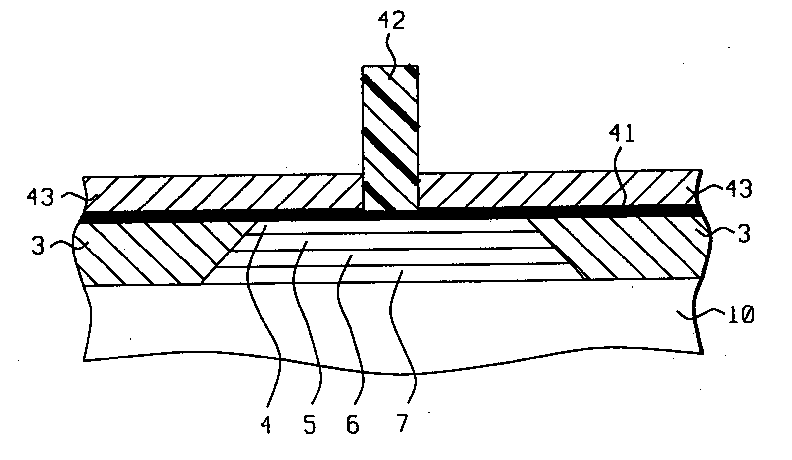
[0020] The process of the present invention starts as illustrated in FIG. 4A. Prior provision of a spin valve structure of the type discussed above is assumed. This includes layers 3 through 7 as shown in FIG. 4A. Additionally, there is a protective layer 41 on the top surfaces of both layers 3 and 4, which layers have been planarized so that their topmost surfaces are coplanar. Layer 41 is typically about 1-30 Angstroms thick and is made of tantalum or ruthenium. Layer 41 will also serve as a seed layer for the electroplating step that occurs later in the process.

[0021] A layer of a patternable resist material is then deposited onto protective layer 41. This resist material may be sensitive to either deep ultraviolet (UV), which we will define here as radiation in the wavelength range of from 1,930 to 2,480 Angstroms or to electron beam radiation. The resist is deposited to a thickness between about 0.5 and 1 microns. After exposure to (and development of) a suitable pattern of th...


PUM

PropertyMeasurementUnit
thickaaaaaaaaaa
thickaaaaaaaaaa
thickaaaaaaaaaa

Abstract

A major problem in Lead Overlay design for GMR structures is that the magnetic read track width is wider than the physical read track width. This is due to high interfacial resistance between the leads and the GMR layer which is an unavoidable side effect of prior art methods. The present invention uses electroplating preceded by a wet etch to fabricate the leads. This approach requires only a thin protection layer over the GMR layer to ensure that interface resistance is minimal. Using wet surface cleaning avoids sputtering defects and plating is compatible with this so the cleaned surface is preserved Only a single lithography step is needed to define the track since there is no re-deposition involved.

Description

FIELD OF THE INVENTION [0001] The invention relates to the general field of magnetic disk storage with particular reference to reading very high track densities BACKGROUND OF THE INVENTION [0002] The principle governing the operation of the read sensor in a magnetic disk storage device is the change of resistivity of certain materials in the presence of a magnetic field (magneto-resistance). Magneto-resistance can be significantly increased by means of a structure known as a spin valve. The resulting increase (known as Giant magneto-resistance or GMR) derives from the fact that electrons in a magnetized solid are subject to significantly less scattering by the lattice when their own magnetization vectors (due to spin) are parallel (as opposed to anti-parallel) to the direction of magnetization of the solid as a whole. [0003] The key elements of a spin valve structure are shown in FIG. 1. Seen there, on substrate 10, is exchange pinning layer 7, made of PtMn or NiMn and having a thic...

Claims


Application Information

Patent Timeline
Patent Type & Authority Applications(United States)
IPC IPC(8): G11B5/127H04R31/00C25D5/02G11B5/31G11B5/39
CPCB82Y10/00G11B5/3116G11B5/3163G11B5/3903Y10T29/49048Y10T29/49021Y10T29/49041Y10T29/49128Y10T29/49044Y10T29/49032Y10T29/49046Y10T29/49052
Inventor CHEN, CHAO-PENGLIN, KEVINCHANG, JEI-WEIJU, KOCHANWANG, HUI-CHUAN
Owner HEADWAY TECH INC
Why Eureka
Try Eureka