Substrate cleaning method and developing apparatus

a technology of developing apparatus and substrate, which is applied in the direction of photomechanical apparatus, cleaning using liquids, instruments, etc., can solve the problems of reducing the width of the resist pattern, the inability of the spin cleaning method to completely remove the dissolution product, and the possibility of residual dissolution product producing development defects, etc., to achieve the effect of reducing the amount of foreign matter remaining on the surface of the substrate, reducing the amount of foreign matter remaining on the substrate, and reducing the defect o

Active Publication Date: 2006-03-09
TOKYO ELECTRON LTD
View PDF5 Cites 81 Cited by
  • Summary
  • Abstract
  • Description
  • Claims
  • Application Information

AI Technical Summary

Benefits of technology

[0010] The present invention has been made in view of such problems and it is therefore an object of the present invention to provide a cleaning method of cleaning the surface of a substrate processed by a developing process that develops an exposed film formed on the substrate by wetting the exposed film with a developer, capable of exercising a high cleaning effect and of accomplishing a cleaning process in a short time, and to provide a cleaning apparatus for carrying out the cleaning method.
[0025] The present invention pours the cleaning liquid onto a central part of the rotating substrate processed by the developing process to form a film of the cleaning liquid over the surface of the substrate, creates the dry area in the central part of the substrate, and rotates the substrate at a rotating speed not lower than 1500 rpm to expand the dry area radially by centrifugal force. Thus the dissolved product produced by the developing process can be very effectively removed, the amount of foreign matters remaining on the surface of the substrate can be reduced, and defects produced by the developing process and remaining on the substrate can be reduced. It is inferred that such an effect of reducing defects produced by the developing process and remaining on the substrate owes to the rapid, forcible radially outward run of a marginal part of the cleaning liquid film contiguous with the margin of the dry area, and the high capability of the marginal part of the cleaning liquid film for carrying the dissolution product away together with the cleaning liquid.
[0026] The dry area can be created in the central area more surely when the gas is blown onto the central part of the substrate after radially spreading the cleaning liquid poured onto the central part of the substrate in a cleaning liquid film and blowing the gas is stopped instantly than when any gas is not blown onto the central part of the substrate. Consequently, the effect of cleaning an area near the central area can be enhanced.
[0027] When pouring the cleaning liquid is stopped at a position at a position inside the peripheral edge of the substrate and at a predetermined distance from the center of the substrate, the disturbance of the cleaning liquid poured onto the substrate by high centrifugal force that acts on the cleaning liquid on the substrate rotating at a high rotating speed not lower than 1500 rpm and hence cleaning effect of the cleaning liquid can be enhanced.

Problems solved by technology

The spin cleaning method, however, is incapable of completely removing the dissolution product.
However, the possibility of the residual dissolution product producing development defects increases with decrease in the width of the component lines of the resist pattern.
Since the resist pattern forming process has many steps, it is desired to reduce the process times of the steps to the shortest possible times. It is hardly possible to ensure perfect cleaning because, in some cases, the dissolution product cannot be completely removed even if the wafer is cleaned for a long cleaning time.
When nitrogen gas is blown onto the gas flowing position behind the liquid pouring position onto which the cleaning liquid is poured as the liquid pouring position is shifted radially, the flow of the cleaning liquid is disturbed by the nitrogen gas, and particles separated from the surface of the wafer W are unable to flow together with the cleaning liquid and remain on the wafer W. Although this known cleaning method is more effective than the spin cleaning method, this known cleaning method has difficulty in exercising a high cleaning effect.

Method used


Image

  • Substrate cleaning method and developing apparatus
  • Substrate cleaning method and developing apparatus
  • Substrate cleaning method and developing apparatus

Examples


first embodiment

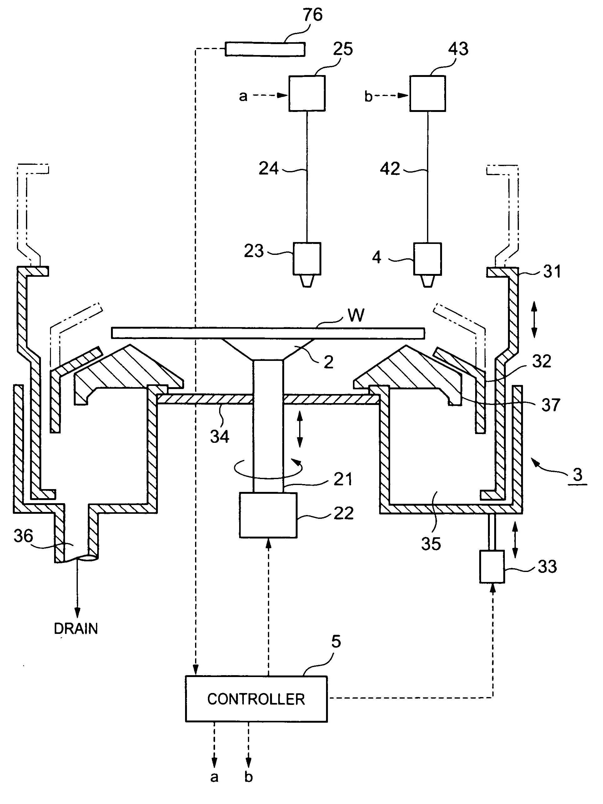
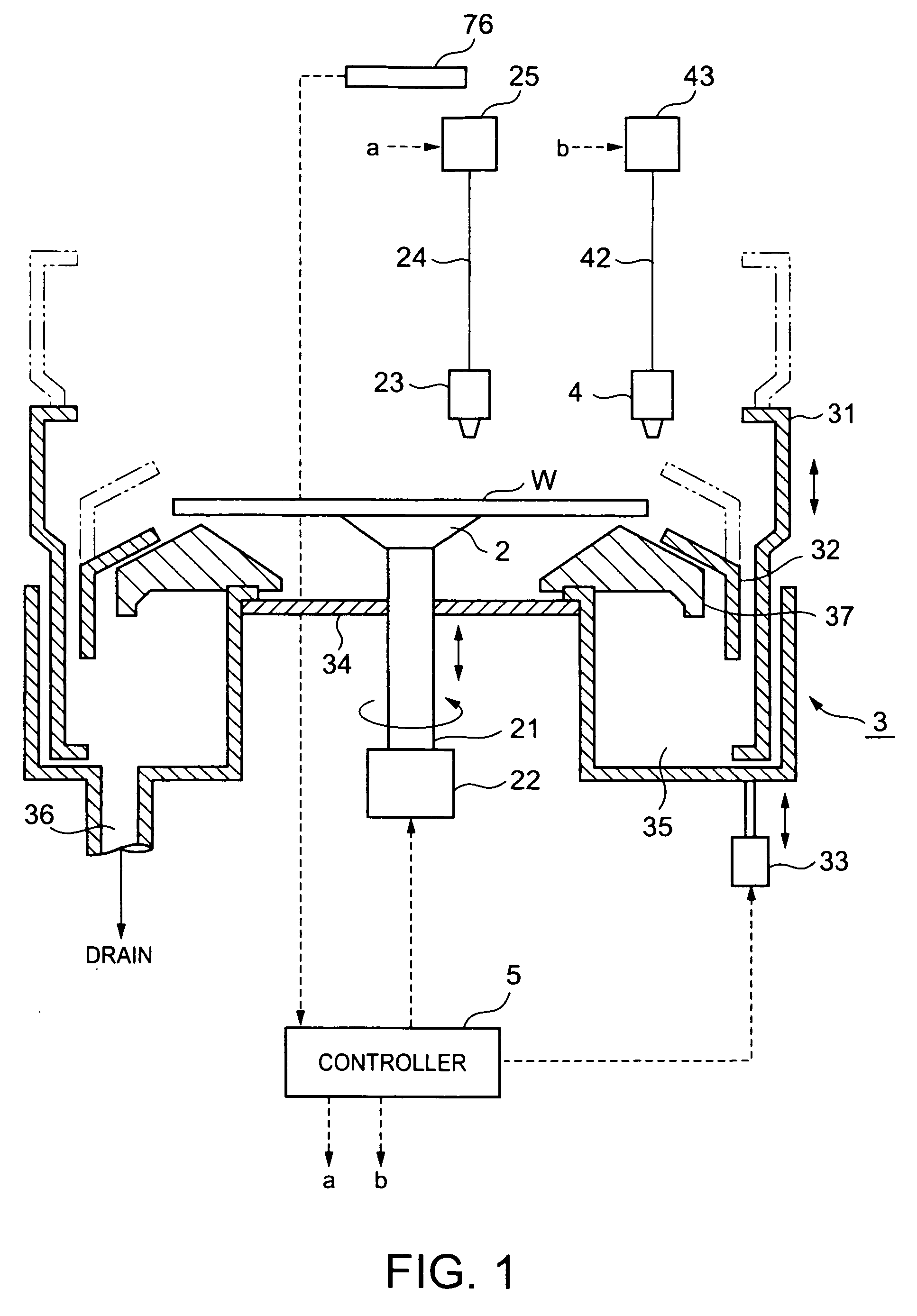
[0041] A developing apparatus in a first embodiment according to the present invention will be described with reference to FIGS. 1 and 2. Indicated at 2 in FIGS. 1 and 2 is a spin chuck, namely, a substrate holding device, for holding, for example, a wafer W, namely, a substrate, by suction in a horizontal position. The spin chuck 2 has a shaft 21 interlocked with a driving mechanism 22 including a rotative mechanism. The spin chuck 2 holding the wafer W is able to rotate and to move vertically. The wafer W is held by the spin chuck 2 coaxially with the shaft 21 of the spin chuck 2.

[0042] A cup device 3 opening upward surrounds the wafer W held on the spin chuck 2. The cup device 3 has an outer cup 31 having a rectangular upper part and a cylindrical lower part, and an inner cup 32 having a tapered upper part tapering upward. A lifting device 33 is connected to the lower end of the outer cup 31 to move the outer cup 31 vertically. A flange formed at the lower end of the outer cup 3...

second embodiment

[0061] A developing apparatus in a second embodiment according to the present invention differs from the developing apparatus in the first embodiment in being provided with a gas blowing nozzle 7 in addition to components like those of the developing apparatus in the first embodiment. As shown in FIG. 6, the gas blowing nozzle 7 may be held together with a cleaning liquid pouring nozzle 4 on a common arm for movement together with the cleaning liquid pouring nozzle 4 or the cleaning liquid pouring nozzle 4 and the gas blowing nozzle 7 may be separately moved. In FIG. 6, the gas blowing nozzle 7 and the cleaning liquid pouring nozzle 4 are fixedly connected by a support member 71. The gas blowing nozzle 7 and the cleaning liquid pouring nozzle 4 are spaced about 30 mm apart. For example, a gas supply pipe connects the gas blowing nozzle 7 to a gas supply system 73. The gas supply system 73 includes a gas source, valves, flow regulators and such. The controller 5 controls the gas supp...

third embodiment

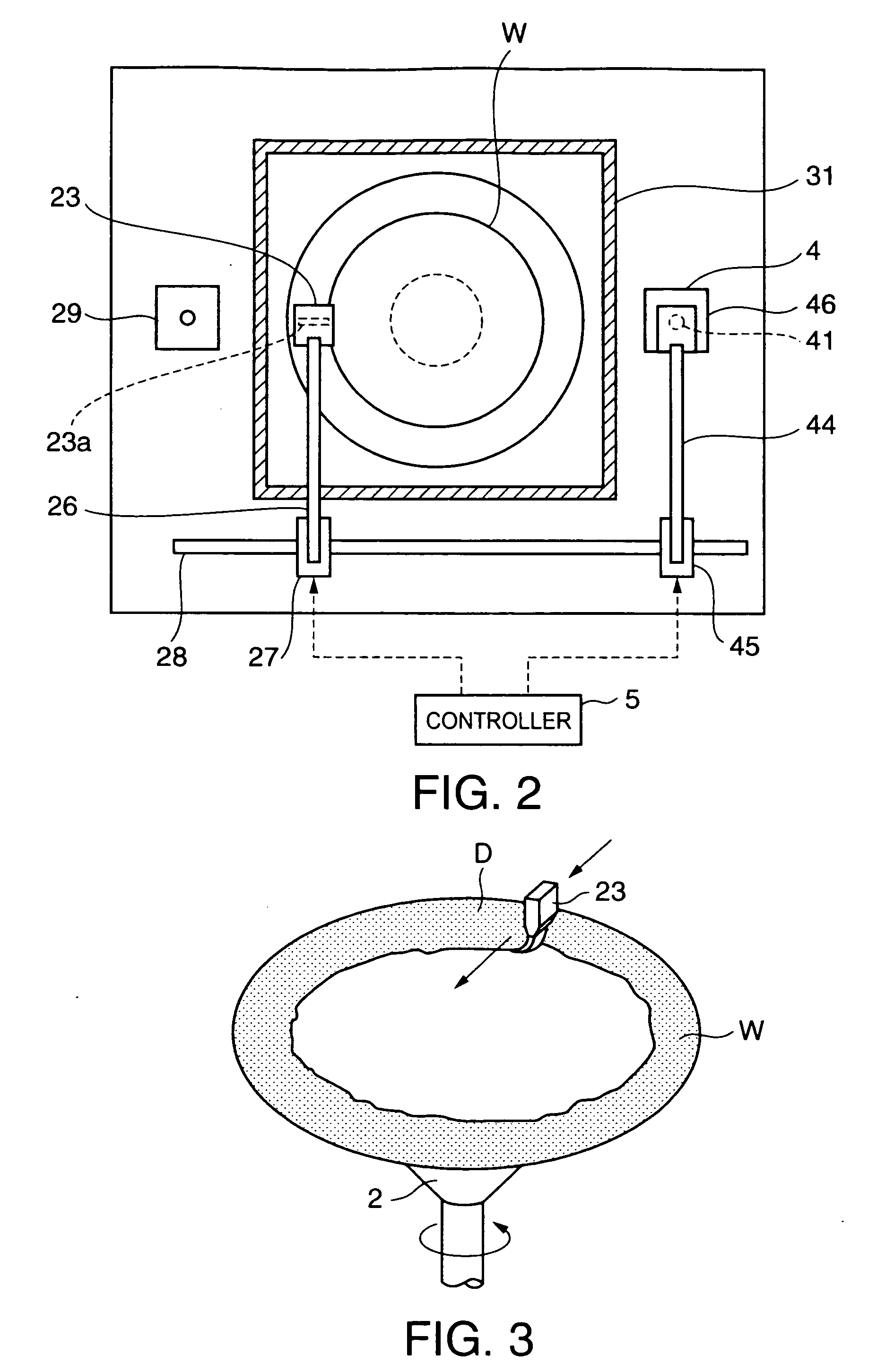
[0069] A developing apparatus in a third embodiment according to the present invention differs from the developing apparatus in the first embodiment in being provided with two cleaning liquid pouring nozzles, namely, a first cleaning liquid pouring nozzle 4 and a second cleaning liquid pouring nozzle 8, pouring a cleaning liquid onto a central part of a wafer W through the first cleaning liquid pouring nozzle 4 and pouring the cleaning liquid onto a part at a predetermined distance from the center of the wafer W. A cleaning process will be described mainly in terms of operations different from those of the first embodiment.

[0070] Step 1: Referring to FIG. 8(a), the first cleaning liquid pouring nozzle 4 and the second cleaning liquid pouring nozzle 8 are disposed at a position corresponding to the center of the wafer W and at a position corresponding to a part of the wafer W, for example, at 80 mm from the center of the wafer W, respectively. Then, the first cleaning liquid pouring...


PUM

PropertyMeasurementUnit
diameteraaaaaaaaaa
distanceaaaaaaaaaa
distanceaaaaaaaaaa

Abstract

A cleaning method highly effectively cleans a surface of a semiconductor wafer by removing a dissolution product, produced when a surface of a semiconductor wafer is processed by a developing process that develops an exposed film formed on the semiconductor wafer by wetting the exposed film with a developer, from the surface of the semiconductor wafer. A cleaning liquid is poured through a cleaning liquid pouring nozzle onto a central part of a rotating wafer processed by a developing process to spread the cleaning liquid in a film over the surface of the wafer. Then, the cleaning liquid pouring nozzle is shifted to create a dry area in a central part of the wafer and the wafer is rotated at 1500 rpm to expand the dry area. The cleaning liquid pouring nozzle is moved at a nozzle moving speed high enough to keep the cleaning liquid pouring position ahead of the margin of the dry area and pouring the cleaning liquid is stopped upon the arrival of the cleaning liquid pouring nozzle at a predetermined position at 80 mm from the center of the wafer or at 5 mm above toward the center of the wafer from the peripheral edge of the wafer. The cleaning liquid may be poured through another cleaning liquid pouring nozzle disposed beforehand at the predetermined position and pouring the cleaning liquid through the cleaning liquid pouring nozzle may be stopped immediately before the margin of the dry area reaches a part onto which the cleaning liquid is poured through the cleaning liquid pouring nozzle. Preferably, a gas is blown instantaneously against the central part of the wafer to form a core fore the dry area.

Description

BACKGROUND OF THE INVENTION [0001] 1. Field of the Invention [0002] The present invention relates to a method of cleaning surfaces of a substrate processed by a developing process which wets the surfaces of the substrate with a developer after exposure, and a developing apparatus for carrying out the method. [0003] 2. Description of the Related Art [0004] A resist pattern forming process is one of semiconductor device fabricating processes. The resist pattern forming process spreads a photoresist over a surface of a semiconductor wafer (hereinafter, referred to simply as “wafer”) in a photoresist film, exposes the photoresist film through a mask of a predetermined pattern, and develops the exposed photoresist film to form a resist pattern. Generally, this resist pattern forming process is carried out by a resist-applying-and-developing system formed by combining an exposure apparatus, and a developing apparatus capable of forming a resist film and of developing the exposed resist fi...

Claims


Application Information

Patent Timeline
Patent Type & Authority Applications(United States)
IPC IPC(8): C23G1/00C03C23/00
CPCB08B3/02H01L21/67051G03F7/3021B08B3/10Y10S134/902H01L21/02057
Inventor NAKAMURA, JUNJIYOSHIHARA, KOUSUKEYAMAMURA, KENTAROIWAO, FUMIKOTAKEGUCHI, HIROFUMI
Owner TOKYO ELECTRON LTD
Why Eureka
Try Eureka