

Solid-state imaging device driving method
- Summary
- Abstract
- Description
- Claims
- Application Information
AI Technical Summary
Benefits of technology
Problems solved by technology
Method used
Image

Examples
Embodiment Construction
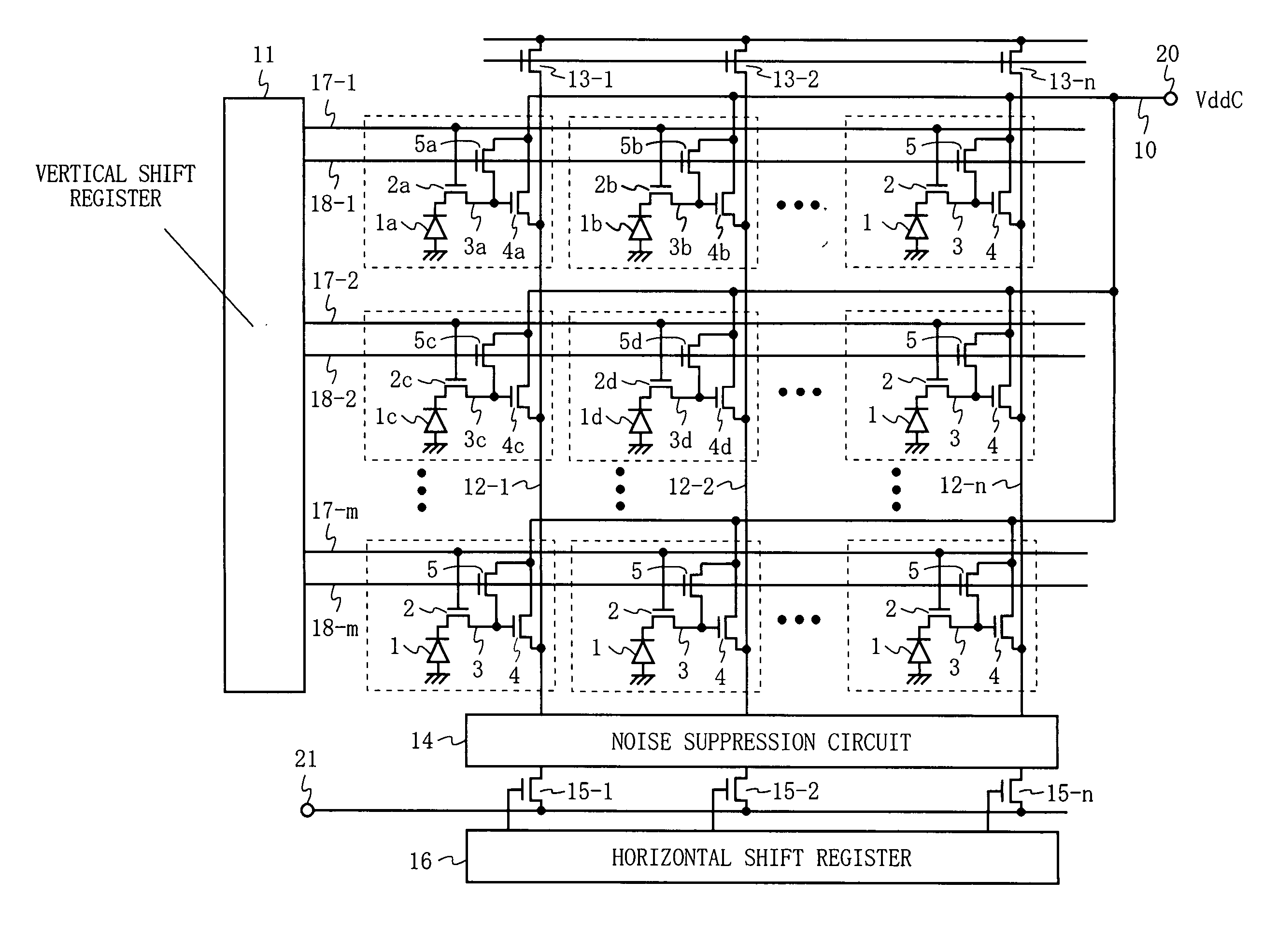
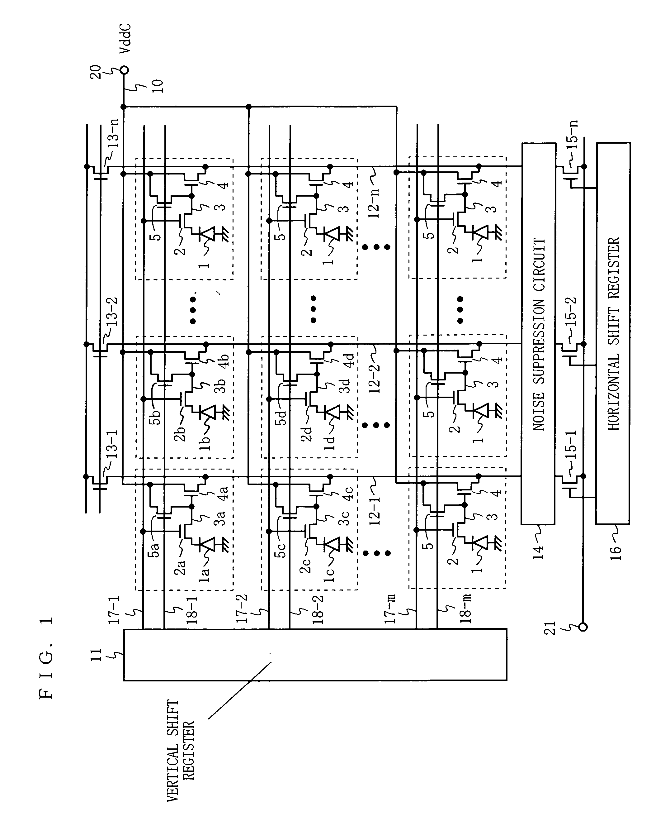
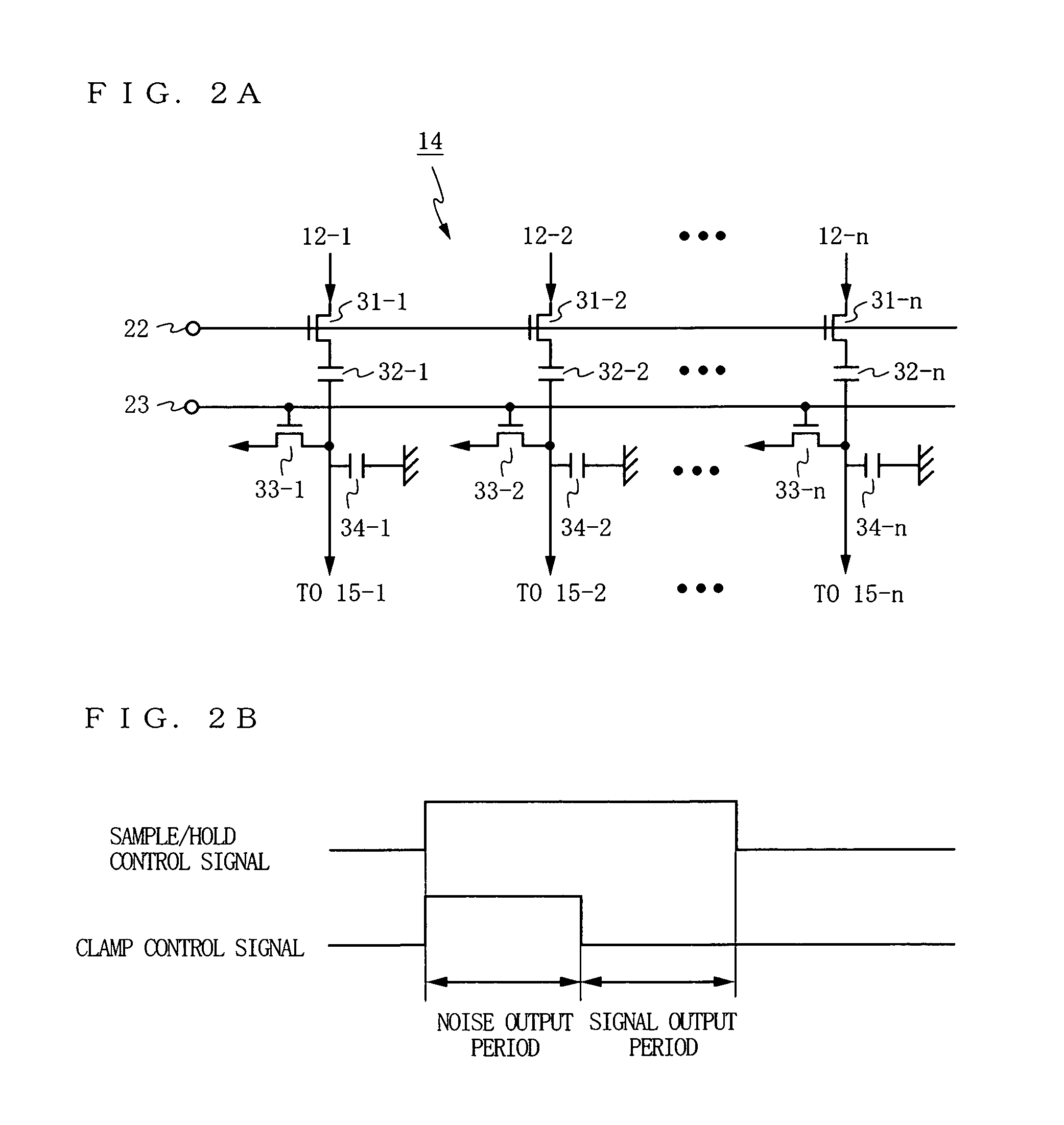
[0028]FIG. 1 is a circuit diagram of a sensor according to an embodiment of the present invention. The sensor shown in FIG. 1 has photosensitive cells (the portions surrounded by dotted-lines) arranged in an m×n matrix form; a power supply line 10; a vertical shift register 11; n vertical signal lines 12-1 to 12-n; n load transistors 13-1 to 13-n; a noise suppression circuit 14; n horizontal transistors; and a horizontal shift register 16. Each photosensitive cell includes a photodiode 1, a transfer gate 2, a floating diffusion layer portion 3, an amplifying transistor 4, and a reset transistor 5. The photosensitive cell is characterized in that it includes three transistors (the transfer gate 2, the amplifying transistor 4, and the reset transistor 5) and does not include an address transistor. The values of m and n in an actual sensor are in the order of from several tens to several thousands.
[0029] The m×n photosensitive cells are formed on a semiconductor substrate. More specif...
PUM
 Abstract
Description
Claims
Application Information