Light-emitting diode

a diode and light-emitting technology, applied in the direction of discharge tube/lamp details, discharge tube luminescnet screens, lighting and heating apparatus, etc., can solve the problems of insufficient luminance, insufficient luminance, and insufficient efficiency of semiconductor light-emitting devices, so as to prevent the leakage of light toward the back, enhance the luminance on the surface in the optical axis direction, and increase the contact area

Inactive Publication Date: 2006-03-09
PANASONIC CORP
View PDF6 Cites 32 Cited by
  • Summary
  • Abstract
  • Description
  • Claims
  • Application Information

AI Technical Summary

Benefits of technology

[0013] An object of the present invention is to provide a high-luminance light-emitting diode capable of emitting light uniformly. Other objects of the present invention are: suppressing removal of components from supporting members such as lead frames; enabling high-density packaging and miniaturization; and enabling emission of light in the same conditions regardless of the orientation of a device.

Problems solved by technology

However, if light-emitting diodes are used under normal conditions, only insufficient luminance is obtained in many cases.
However, the conventional light-emitting diodes have a drawback in which light from a semiconductor light-emitting device is not efficiently released from a light-emitting surface and thus luminance is not enhanced.
Specifically, in the light-emitting diode disclosed in Reference 2, light emitted from the semiconductor light-emitting device toward the sides is released to the outside as it is from the side face of the resin package, resulting in wasting a large amount of light.
However, light emitted from the devices toward the sides is released to the outside from the side face of the resin package, and thus a large amount of light is also wasted.
The conventional light-emitting diodes have another drawback in which light is not uniformly emitted.
The conventional light-emitting diodes have still another drawback in which a resin package is readily disconnected from a supporting member such as a lead frame.
In the conventional light-emitting diodes have yet another drawback in which high-density integration and miniaturization are not implemented.
Specifically, the configuration disclosed in Reference 5 is not applicable to apparatus for surface mounting, so that high-density integration is not achieved.
Therefore, this configuration is not applicable to equipment which needs to be thin.
Therefore, this configuration does not meet miniaturization.
The conventional light-emitting diodes have another drawback in which each light-emitting diode is mounted on a circuit board or the like in a limited orientation depending on the arrangement of lead members.

Method used


Image

  • Light-emitting diode
  • Light-emitting diode
  • Light-emitting diode

Examples


embodiment 1

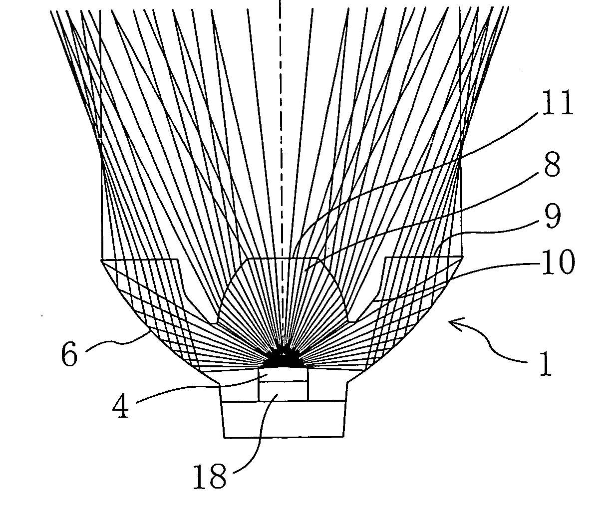
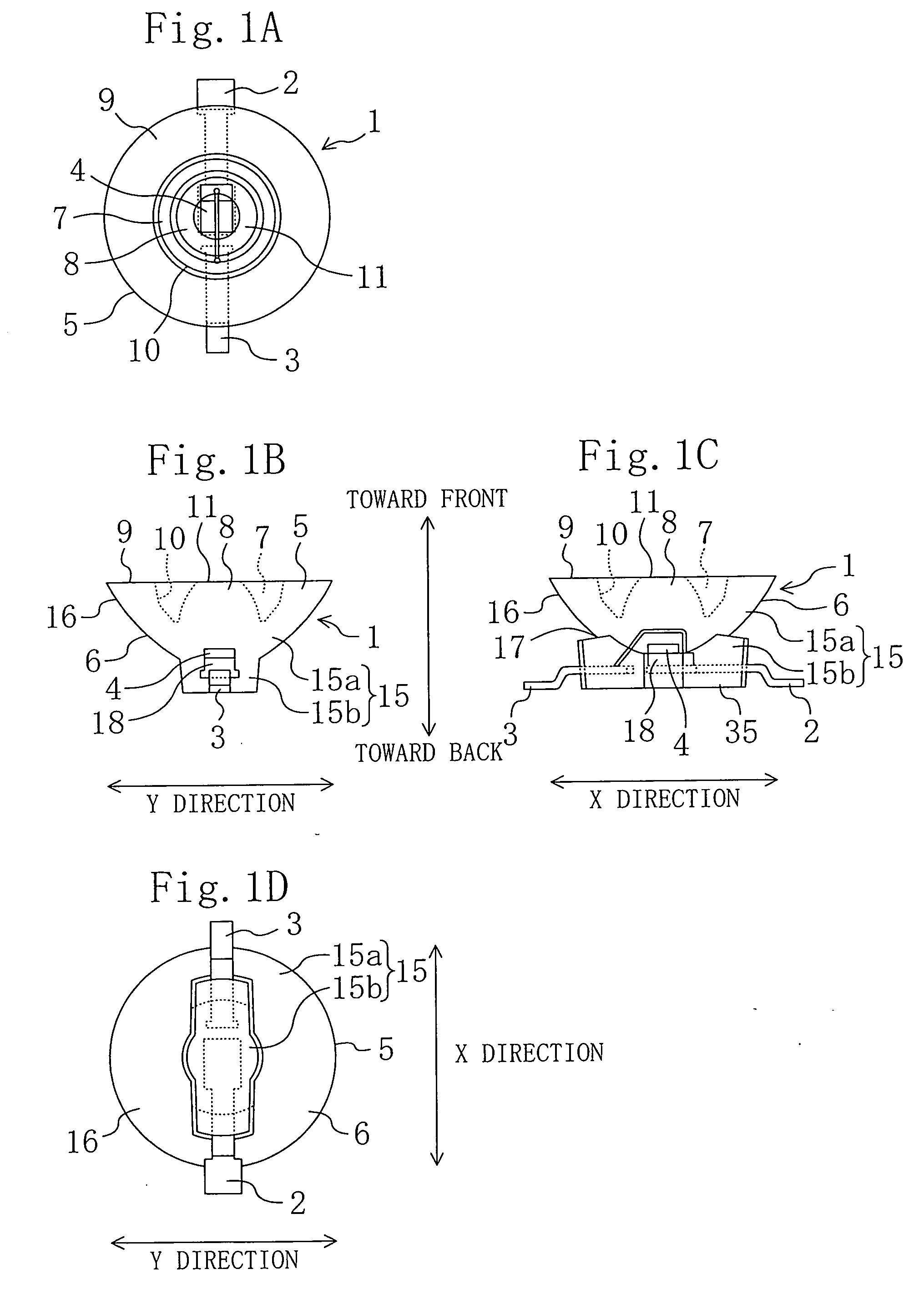
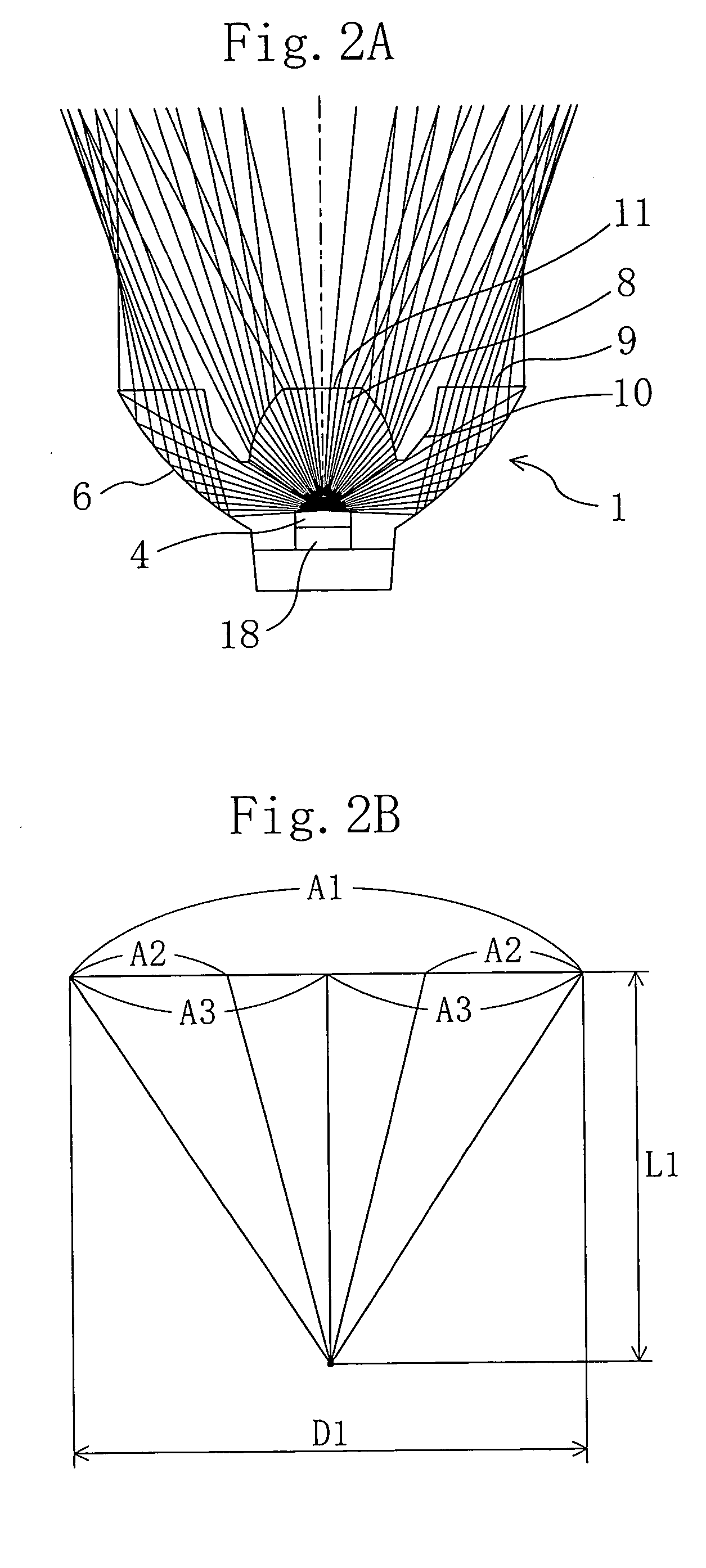
[0055]FIG. 1(A) is a plan view showing a light-emitting diode according to a first embodiment of the present invention. FIG. 1(B) is a front view of the light-emitting diode. FIG. 1(C) is a side view of the light-emitting diode. FIG. 1(D) is a bottom view of the light-emitting diode.

[0056] As shown in FIG. 1, a light-emitting diode 1 includes: a semiconductor light-emitting device 4 mounted over lead frames 2 and 3; and a transparent resin package 5 covering the semiconductor light-emitting device 4.

[0057] The lead frames 2 and 3 are formed by bending, into a gull-wing shape, a plate member obtained by, for example, applying a Ni / Ag coating to a Cu alloy or others. More specifically, the lead frames 2 and 3 extend from base parts thereof over which the semiconductor light-emitting device 4 is mounted, project from both sides of the resin package 5, bend backward and then outward, and extend to the outside at the both sides.

[0058] The semiconductor light-emitting device 4 in the s...

embodiment 2

[0086]FIG. 3(A) is a plan view showing a light-emitting diode according to a second embodiment of the present invention. FIG. 3(B) is a front view of the light-emitting diode. FIG. 3(C) is a side view of the light-emitting diode. FIG. 3(D) is a bottom view of the light-emitting diode.

[0087] A light-emitting diode 22 according to the second embodiment is different from the light-emitting diode 1 of the first embodiment in that two semiconductor light-emitting devices and four lead frames are provided.

[0088] Lead frames 23, 24, 25 and 26 are formed into gull-wing shapes and are arranged close to each other at an end and form a cross. Two semiconductor light-emitting devices 27 and 28 are respectively mounted over the opposed lead frames 23 and 25 by die bonding. The semiconductor light-emitting device 27 is connected to the lead frame 25 by wire bonding. The semiconductor light-emitting device 28 is connected to the lead frame 26 by wire bonding. The centers of the respective semico...

embodiment 3

[0099] In a third embodiment, though not shown, a light-emitting diode in which three semiconductor light-emitting devices are mounted over lead frames will be described. The light-emitting diode according to this embodiment uses semiconductor light-emitting devices emitting red light, green light and blue light, respectively. Each of the semiconductor light-emitting devices can produce one of red, green and blue, a mixture of two of these colors, or a mixture of these three colors. White light can also be produced by adjusting the luminances of the three colors.

[0100] In this embodiment, a circular flat portion is formed on each convex lens portion to diffuse light, so that the luminances of the colors are made uniform and the colors are uniformly mixed.

[0101] White light obtained from blue light by using a yellow phosphor has a small amount of red component. Accordingly, if such white light is used by a flash for taking pictures, white light different from natural light is gener...


PUM


Abstract

A light-emitting diode 1 according to the present invention includes: a semiconductor light-emitting device 4 mounted on the surface of lead frames 2 and 3; and a transparent resin package 5 covering the front side of the semiconductor light-emitting device 4. A convex lens portion 8 for concentrating light emitted from the semiconductor light-emitting device 4 toward the front is provided in a surface part of the resin package 5. A circular flat portion 11 for diffusing light emitted from the semiconductor light-emitting device 4 toward the sides is provided in a part of the convex lens portion 8 intersecting the optical axis of the convex lens portion 8. Part of the convex lens portion 8 surrounding the circular flat portion 11 is a convex-lens side face. A recess 7 whose side wall is partly the convex-lens side face is provided to surround the convex lens portion.

Description

TECHNICAL FIELD [0001] The present invention relates to light-emitting diodes including semiconductor light-emitting devices and transparent resin packages covering the semiconductor light-emitting devices. BACKGROUND ART [0002] In recent years, cellular phones equipped with cameras have become dominant for domestic use, and thus small, thin and bright light sources for flashes capable of taking pictures even in dark places have been required. To meet this requirement, light-emitting diodes (LEDs) are promising. However, if light-emitting diodes are used under normal conditions, only insufficient luminance is obtained in many cases. To avoid this, attempts have been made to provide resin packages covering semiconductor light-emitting devices with a function as lenses. [0003] Examples of use of resin packages as lenses include the following configurations. In Japanese Unexamined Patent Publication (Kokai) No. 1-273367 (pp. 1-4, FIG. 3) (hereinafter referred to as Reference 1), disclo...

Claims


Application Information

Patent Timeline
Patent Type & Authority Applications(United States)
IPC IPC(8): F21V7/04H01L25/075H01L33/54H01L33/58H01L33/60
CPCH01L25/0753H01L33/54H01L2224/48247H01L33/60H01L33/58H01L2224/48095
Inventor IKEDA, TADAAKITOKUTOMI, SHINJIKOGA, NORIAKI
Owner PANASONIC CORP
Why Eureka
Try Eureka