Liquid crystal display device and fabrication method thereof

a technology of liquid crystal display and fabrication method, which is applied in the direction of semiconductor devices, instruments, electrical devices, etc., can solve the problems of increasing fabrication cost and reducing production yield, and achieve the effect of simplifying the method of fabrication and reducing the number of mask processes used to fabricate array substrates

Inactive Publication Date: 2006-03-09
LG DISPLAY CO LTD
View PDF5 Cites 11 Cited by
  • Summary
  • Abstract
  • Description
  • Claims
  • Application Information

AI Technical Summary

Benefits of technology

[0021] An advantage of the present invention provides an LCD device and a method of fabricating the same wherein the number of mask processes used to fabricate an array substrate is reduced.
[0022] Another advantage of the present invention provides an LCD device having a storage capacitor and a simplified method of fabricating the same.
[0023] Additional features and advantages of the invention will be set forth in the description which follows, and in part will be apparent from the description, or may be learned by practice of the invention. These and other advantages of the invention will be realized and attained by the structure particularly pointed out in the written description and claims hereof as well as the appended drawings.
[0024] To achieve these and other advantages and in accordance with the purpose of the present invention, as embodied and broadly described, a method for fabricating a liquid crystal display device may, for example, include providing a first substrate; forming an active layer on the first substrate, wherein the active layer includes a source region, a drain region, a channel region, and a storage region; forming a first insulation film on the first substrate; forming a gate electrode, a gate line, a pixel electrode, and a storage line on the substrate, wherein storage line overlaps the storage region; forming a second insulation layer on the first substrate; forming first and second contact holes through the first and second insulation layers, wherein the first and second contact holes expose respective ones of the source and drain regions; forming a pixel hole through the second insulation layer, wherein the pixel hole exposes the pixel electrode; forming a source electrode electrically connected to the source region through the first contact hole and a drain electrode electrically connected to the drain region through the second contact hole; bonding a second substrate to the first substrate; and providing a layer of liquid crystal between the first and second substrates.
[0025] In another aspect of the present invention, a liquid crystal display (LCD) device may, for example, include first and second substrates; an active layer formed as a silicon layer on the first substrate, the active layer having a storage region; a first insulation layer on the first substrate; a gate electrode and a gate line having first and second conductive layers; a storage line partially overlapping a the storage region; a pixel electrode having the first conductive layer; a second insulation layer opening the pixel electrode, the second insulation layer having first and second contact holes; a source electrode connected with a source region through the first contact hole and a drain electrode connected with a drain region through the second contact hole; and a liquid crystal layer between the first and second substrates.
[0026] It is to be understood that both the foregoing general description and the following detailed description are exemplary and explanatory and are intended to provide further explanation of the invention as claimed.

Problems solved by technology

Thus, any method of fabricating array substrates that uses a large amount of photolithographic processes may result in a reduced production yield and increase the cost of fabrication.

Method used


Image

  • Liquid crystal display device and fabrication method thereof
  • Liquid crystal display device and fabrication method thereof
  • Liquid crystal display device and fabrication method thereof

Examples


first embodiment

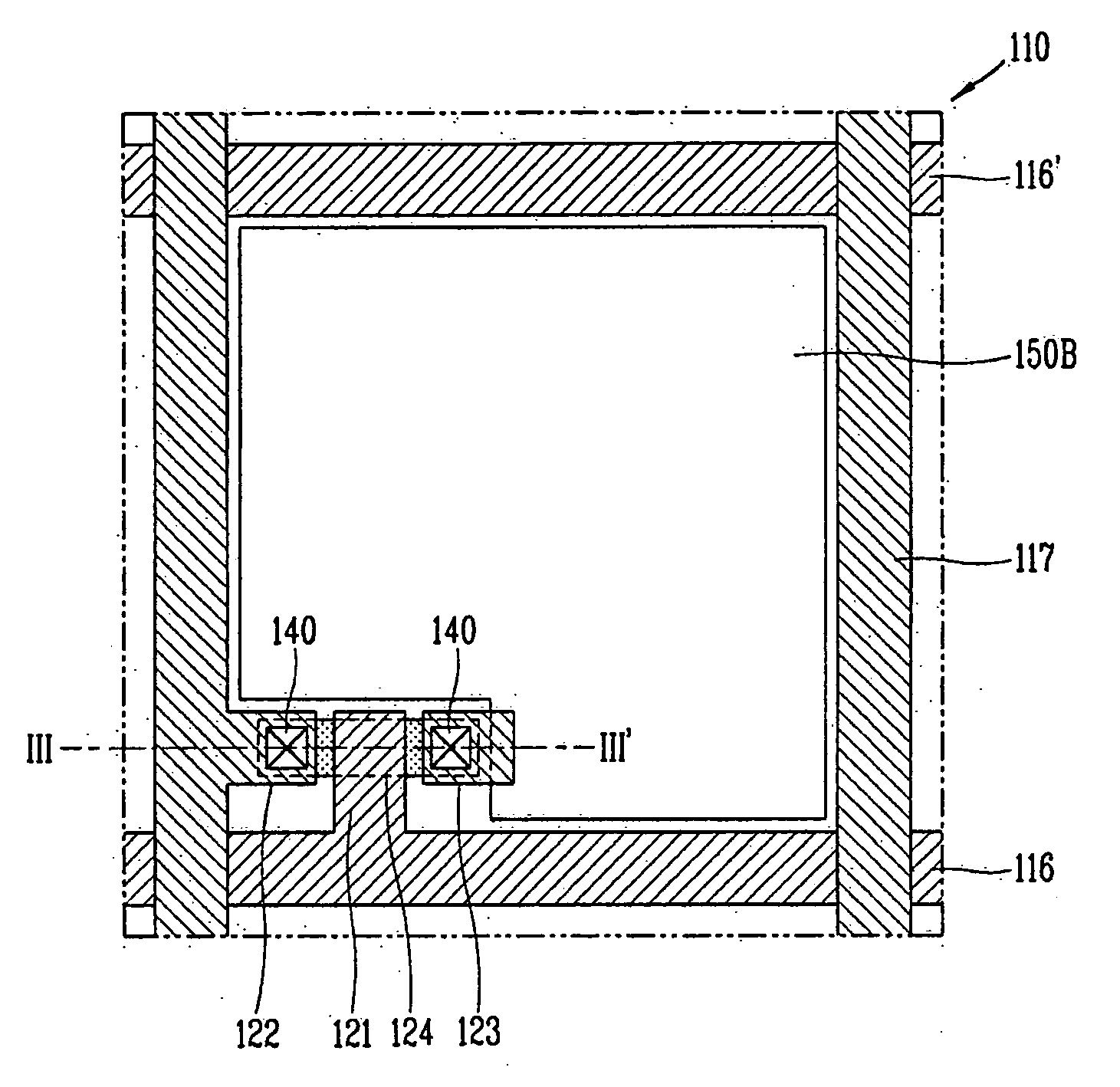
[0040] Referring to FIG. 3, the array substrate 110 according to principles of the present invention may, for example, support horizontally oriented gate lines 116 and 116′ and vertically oriented data lines 117 defining a pixel region. According to principles of the present invention, and with respect to a particular pixel, reference numeral 116 designates the gate line that is connected to a corresponding TFT while reference numeral 116′ designates a gate line that merely defines an edge of the pixel region. A switching device such as a TFT may be formed at the crossing of a gate line 116 and a corresponding data line 117 and a pixel electrode 150B may be formed within each pixel region. In one aspect of the present invention, each pixel electrode may be connected with a corresponding TFT and, in concert with a common electrode, may drive a layer of liquid crystal provided within the pixel region.

[0041] Each TFT may, for example, include a gate electrode 121 connected to the gate ...

second embodiment

[0061]FIG. 6 illustrates a partial plan view of an array substrate according to principles of the present invention.

[0062] Referring generally to FIG. 6, the principles of the second embodiment of the present invention may exemplarily provide an array substrate identical to the array substrate of the first embodiment but further including a storage-on-common (SOC) structure, wherein a storage capacitor is formed within the pixel region using a storage line. Thus, and with the exception of the storage capacitor, the array substrate of the second embodiment may be fabricated identically to the array substrate of the first embodiment.

[0063] The array substrate 210 according to principles of the second embodiment of the present invention may, for example, support horizontally oriented gate lines 216 and 216′ and vertically oriented data lines 217 defining a pixel region. According to principles of the present invention, and with respect to a particular pixel, reference numeral 216 desi...

third embodiment

[0066]FIG. 7 illustrates a partial plan view of an array substrate according to principles of the present invention.

[0067] Referring to FIG. 7, the array substrate 310 according to principles of the third embodiment of the present invention may, for example, support horizontally oriented gate lines 316 and 316′ and vertically oriented data lines 317 defining a pixel region. According to principles of the present invention, and with respect to a particular pixel, reference numeral 316 designates the gate line that is connected to a corresponding TFT while reference numeral 316′ designates a gate line that merely defines an edge of the pixel region. A switching device such as a TFT may be formed at the crossing of a gate line 316 and a corresponding data line 317 and a pixel electrode 350B may be formed within each pixel region. In one aspect of the present invention, each pixel electrode 350B may be connected with a corresponding TFT and, in concert with a common electrode, may drive...


PUM


Abstract

A method for fabricating a liquid crystal display device includes providing first and second substrates; forming an active layer on the first substrate, wherein the active layer includes a source region, a drain region, a channel region, and a storage region; forming a first insulation layer on the first substrate; forming a gate electrode, a gate line, a pixel electrode, and a storage line on the first substrate, wherein storage line overlaps the storage region; forming a second insulation layer on the first substrate; forming first and second contact holes through the first and second insulation layers, wherein the first and second contact holes expose respective ones of the source and drain regions; forming a pixel hole through the second insulation layer, wherein the pixel hole exposes the pixel electrode; forming a source electrode electrically connected to the source region through the first contact hole and a drain electrode electrically connected to the drain region through the second contact hole; and forming a liquid crystal layer between the first and second substrates.

Description

[0001] This application claims the benefit of Korean Patent Application No. P2004-72254, filed on Sep. 9, 2004, which is hereby incorporated by reference for all purposes as if fully set forth herein. BACKGROUND OF THE INVENTION [0002] 1. Field of the Invention [0003] The principles of the present invention generally relate to liquid crystal display (LCD) devices and their methods of fabrication. More particularly, the principles of the present invention relate to an LCD device having a storage capacitor and a simplified method of fabricating the same. [0004] 2. Discussion of the Related Art [0005] As demand for information displays and applications for portable information devices increase, thin film type flat panel display (FPD) devices have been actively researched and developed. Of the various types of FPD devices, LCD devices are particularly beneficial as the LCD panels provided therein express images at high resolution and excellent color quality. Accordingly, LCD devices are...

Claims


Application Information

Patent Timeline
Patent Type & Authority Applications(United States)
IPC IPC(8): H01L21/00
CPCG02F1/136213H01L27/14621G02F1/136227G02F1/136
Inventor PARK, YONG INLEE, DEA YUU
Owner LG DISPLAY CO LTD
Why Eureka
Try Eureka