Atomic layer deposition of metal oxynitride layers as gate dielectrics

a technology of metal oxynitride and gate dielectric, which is applied in the direction of basic electric elements, electrical apparatus, and semiconductor devices, etc., can solve the problems of increased output and undesirable leakage currents, and achieve the undesirable level of 1 a/cmsup>2, 2 /sub>

Inactive Publication Date: 2006-03-09
AHN KIE Y +1
View PDF14 Cites 396 Cited by
  • Summary
  • Abstract
  • Description
  • Claims
  • Application Information

AI Technical Summary

Benefits of technology

[0014]FIG. 1 is a cross-sectional view of a field effect transistor device of the prior art;

Problems solved by technology

Smaller channel lengths require reduced operating voltages, which result in decreased output.
SiO2 is commonly used as a gate dielectric material because it has superior isolation qualities, forms a thermodynamically and electrically stable interface with silicon, and can be applied in a layer as thin as 15 Å. However, if the thickness of SiO2 gate dielectric 12 is decreased below 15 Å, leakage currents exceed an undesirable level of 1 A / cm2 at 1V.
Using Ta2O5, SrTiO3, or Al2O3 is problematic because they are not thermodynamically stable with silicon (they react with silicon to form an undesirable oxide layer).
Using ZrO2 or HfO2 is also problematic because at the temperatures necessary for their deposition, the semiconductor substrate 2 oxidizes and forms an oxide layer at an interface between the semiconductor substrate 2 and the gate dielectric 12.
This oxide layer increases the effective thickness of the metal oxide and reduces its effectiveness as a gate dielectric material.
In addition, the oxide layer has a weak resistance to oxygen diffusion, causing growth of interfacial SiO2 during high temperature annealing.
In addition, ZrO2 layers react with the polysilicon in the gate 10 and cause an increase in leakage current.

Method used


Image

  • Atomic layer deposition of metal oxynitride layers as gate dielectrics
  • Atomic layer deposition of metal oxynitride layers as gate dielectrics

Examples


example 1

Formation of the ZrON Layer by ALD

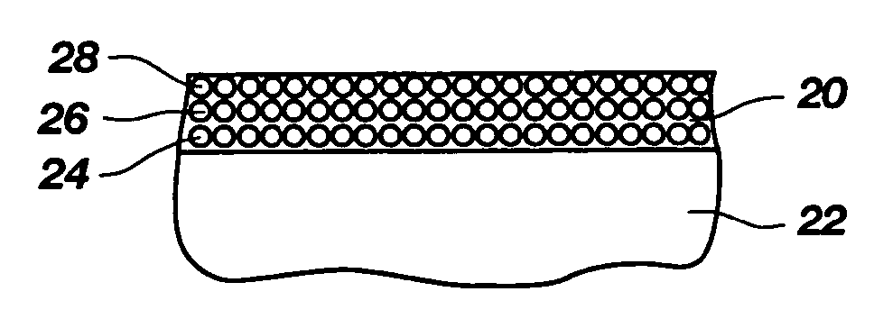
[0032] A semiconductor substrate 22 that has been previously etched in hydrofluoric acid to remove native SiO2 is placed in a hot-wall horizontal flow-type ALD reactor. The pressure in the ALD reactor is maintained at approximately 250 Pa. ZrI4 is evaporated in an open boat inside the ALD reactor, which is maintained at 240° C. The evaporated ZrI4 is transported from one side of a reactor zone of the ALD reactor to the other side to form the zirconium monolayer on the surface of the semiconductor substrate. After purging the ZrI4 for approximately two seconds, H2O—H2O2 vapor, which is generated in an external reservoir at room temperature, is introduced into the ALD reactor through needle and solenoid valves to form the oxide monolayer. After purging the H2O—H2O2 vapor for approximately two seconds, t-BuNH2 or allylNH2 is introduced into the ALD reactor through needle and solenoid valves to form the nitride monolayer. Optionally, NH3 is introduced ...


PUM

PropertyMeasurementUnit
pressureaaaaaaaaaa
pressureaaaaaaaaaa
pressureaaaaaaaaaa

Abstract

A metal oxynitride layer formed by atomic layer deposition of a plurality of reacted monolayers, the monolayers comprising at least one each of a metal, an oxide and a nitride. The metal oxynitride layer is formed from zirconium oxynitride, hafnium oxynitride, tantalum oxynitride, or mixtures thereof. The metal oxynitride layer is used in gate dielectrics as a replacement material for silicon dioxide. A semiconductor device structure having a gate dielectric formed from a metal oxynitride layer is also disclosed.

Description

CROSS-REFERENCE TO RELATED APPLICATION [0001] This application is a continuation of application Ser. No. 10 / 352,507, filed Jan. 27, 2003, pending.FIELD OF THE INVENTION [0002] The present invention relates to a semiconductor device structure and a method for forming the same and, more specifically, to a metal oxynitride gate dielectric and a method for forming the metal oxynitride gate dielectric using atomic layer deposition. BACKGROUND OF THE INVENTION [0003] Silicon dioxide (“SiO2”) has been used as a material to form gate dielectrics, which are used in many semiconductor devices such as field effect transistor (“FET”) devices. The FET is an active device used in complementary metal oxide semiconductor (“CMOS”) integrated circuit technology. As shown in FIG. 1, a conventional FET device includes a semiconductor substrate 2 having a channel 4 that is electrically connected to a source 6 and drain 8. When a voltage difference is present between the source 6 and drain 8, current flo...

Claims


Application Information

Patent Timeline
Patent Type & Authority Applications(United States)
IPC IPC(8): H01L21/336H01L21/31H01L21/3205H01L21/8242H01L21/28H01L21/314H01L29/51
CPCH01L21/28202H01L21/3141H01L21/28194H01L29/513H01L29/518H01L21/3143H01L21/02175H01L21/0228
Inventor AHN, KIE Y.FORBES, LEONARD
Owner AHN KIE Y
Why Eureka
Try Eureka