Eureka AIR delivers breakthrough ideas for toughest innovation challenges, trusted by R&D personnel around the world.

Bipolar transistor with high dynamic performances

Active Publication Date: 2006-03-16
STMICROELECTRONICS SRL
View PDF4 Cites 6 Cited by
  • Summary
  • Abstract
  • Description
  • Claims
  • Application Information

AI Technical Summary

Benefits of technology

[0009] An object of the present invention is to provide a bipolar transistor with improved dynamic performances.
[0010] Another object of the present invention is to provide a bipolar transistor which is easily integrable in a Bi-CMOS process.

Problems solved by technology

The parameters which modify the current gain of bipolar transistors are in a greater number, sometimes poorly understood and often poorly controlled.

Method used


Image

  • Bipolar transistor with high dynamic performances
  • Bipolar transistor with high dynamic performances
  • Bipolar transistor with high dynamic performances

Examples


Embodiment Construction

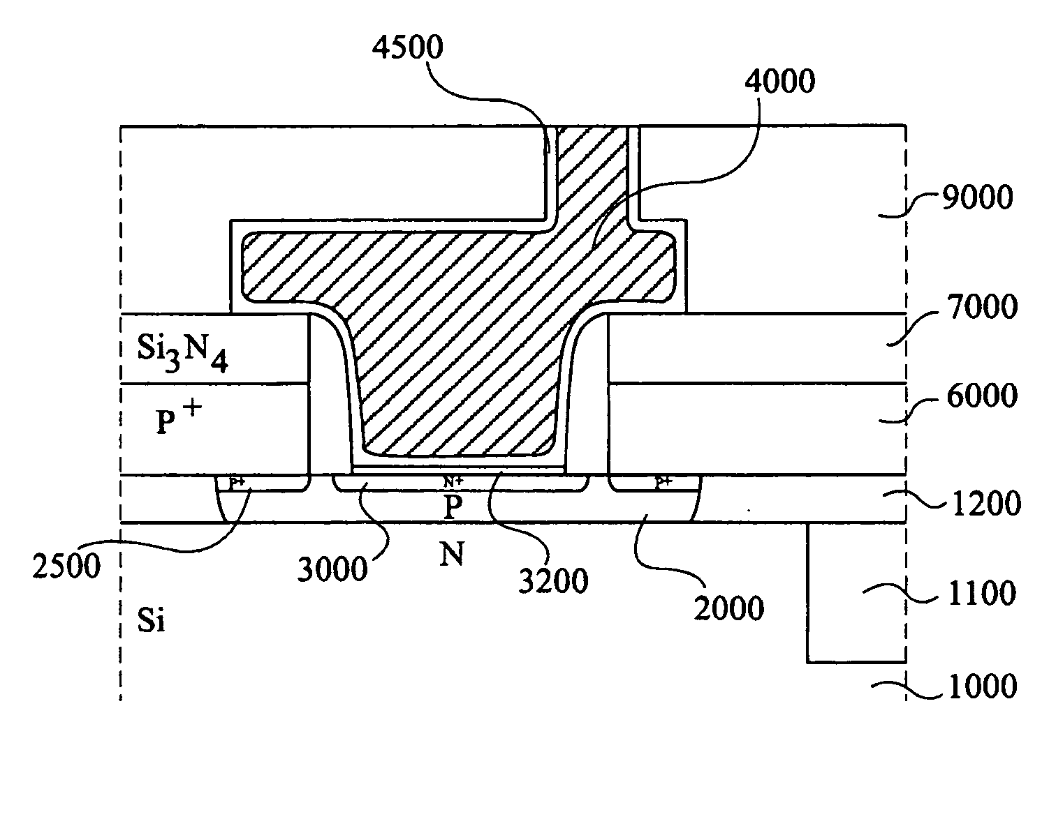
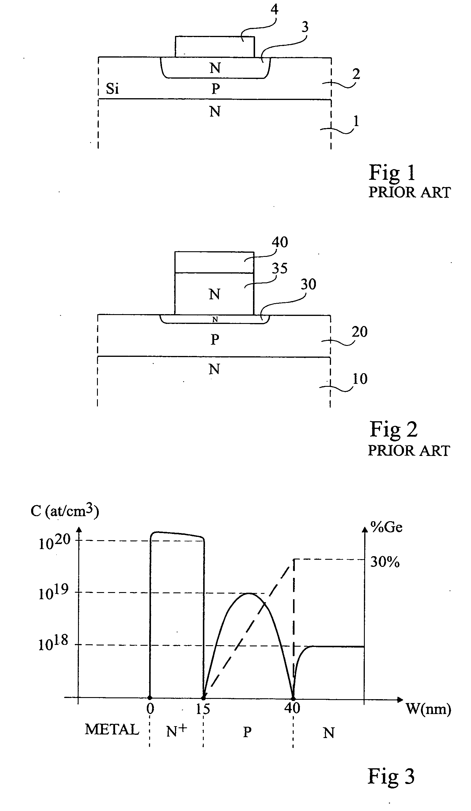
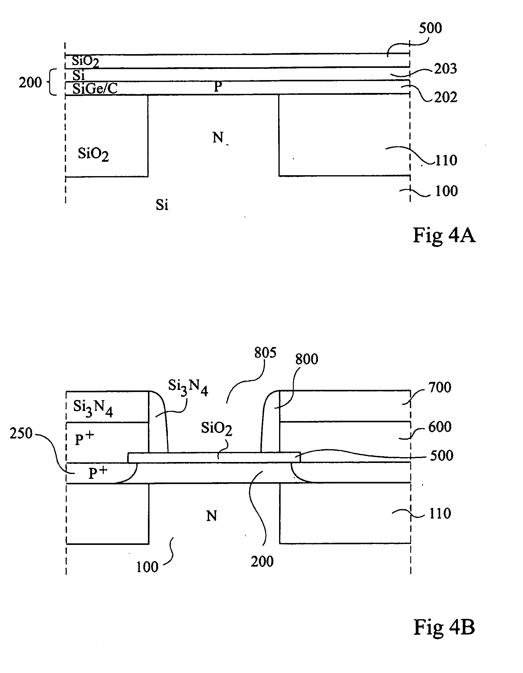
[0031] As usual in the representation of integrated circuit devices, the scales are not respected to better show the different layers and elements of the devices.

[0032] According to the present invention, to increase the dynamic performances of a bipolar transistor, the applicant uses a bipolar transistor, the single-crystal silicon emitter of which has a thickness smaller than 50 nm. It is preferable, to optimize the dynamic performances, to use a thickness for the emitter region ranging between 5 and 30 nm.

[0033] Such a transistor, for example, of type NPN, comprises an N-type doped single-crystal silicon collector region on which is formed by epitaxial growth a single-crystal silicon base region in which is formed an emitter region. The base region is P-type doped, for example, with boron. At the surface of this base, and inside thereof, there exists a heavily-doped N-type region which forms the emitter region of the bipolar transistor. A metal rests on this emitter, forming a ...


PUM


Abstract

A novel bipolar transistor with very high dynamic performances, usable in an integrated circuit. This bipolar transistor comprises a single-crystal silicon emitter region with a thickness smaller than 50 nm. The base of the bipolar transistor is made of an SiGe alloy.

Description

BACKGROUND OF THE INVENTION [0001] 1. Field of the Invention [0002] The present invention relates to the field of microelectronics, and more specifically to a bipolar transistor and to its implementation. [0003] 2. Discussion of the Related Art [0004] Bipolar transistors used as integrated circuit components especially likely to cohabit with MOS transistors in integrated circuits of Bi-CMOS type will more specifically be considered herein. [0005] Integrated circuits with increasingly high performances are developed. To achieve this, all components must be optimized. Bipolar transistors are used on behalf of their dynamic performances which enable their use in the field of very high frequencies, greater than 50 GHz. [0006] A conventional NPN-type transistor is schematized in FIG. 1. It comprises an N-type doped single-crystal silicon collector region 1, a P-type doped single-crystal silicon base region 2, and an N-type doped single-crystal silicon emitter region 3. The collector is f...

Claims


Application Information

Patent Timeline
IPC IPC(8): H01L27/082H01L21/28H01L21/331H01L21/8222H01L21/8248H01L21/8249H01L27/06H01L29/08H01L29/36H01L29/417H01L29/423H01L29/45H01L29/737
CPCH01L21/8249H01L29/0817H01L29/36H01L29/7378H01L29/42304H01L29/456H01L29/66242H01L29/41708
Inventor CHANTRE, ALAINMARTINET, BERTRANDMARTY, MICHELCHEVALIER, PASCAL
Owner STMICROELECTRONICS SRL
Why Eureka
Eureka Blog
Learn More