

Mask for exposure and method of manufacturing the same
a technology for masks and exposures, applied in the field of masks for exposures and a manufacturing method, can solve problems such as difficult accurate measurement of phase difference, and achieve the effect of improving measurement accuracy and good accuracy
- Summary
- Abstract
- Description
- Claims
- Application Information
AI Technical Summary
Benefits of technology
Problems solved by technology
Method used
Image

Examples
first embodiment
(1) First Embodiment
[0036]FIGS. 2A to 2I are the in-process sectional views of a mask for exposure according to a first embodiment of the present invention.
[0037] First of all, description will be made for process until the sectional structure shown in FIG. 2A will be obtained.
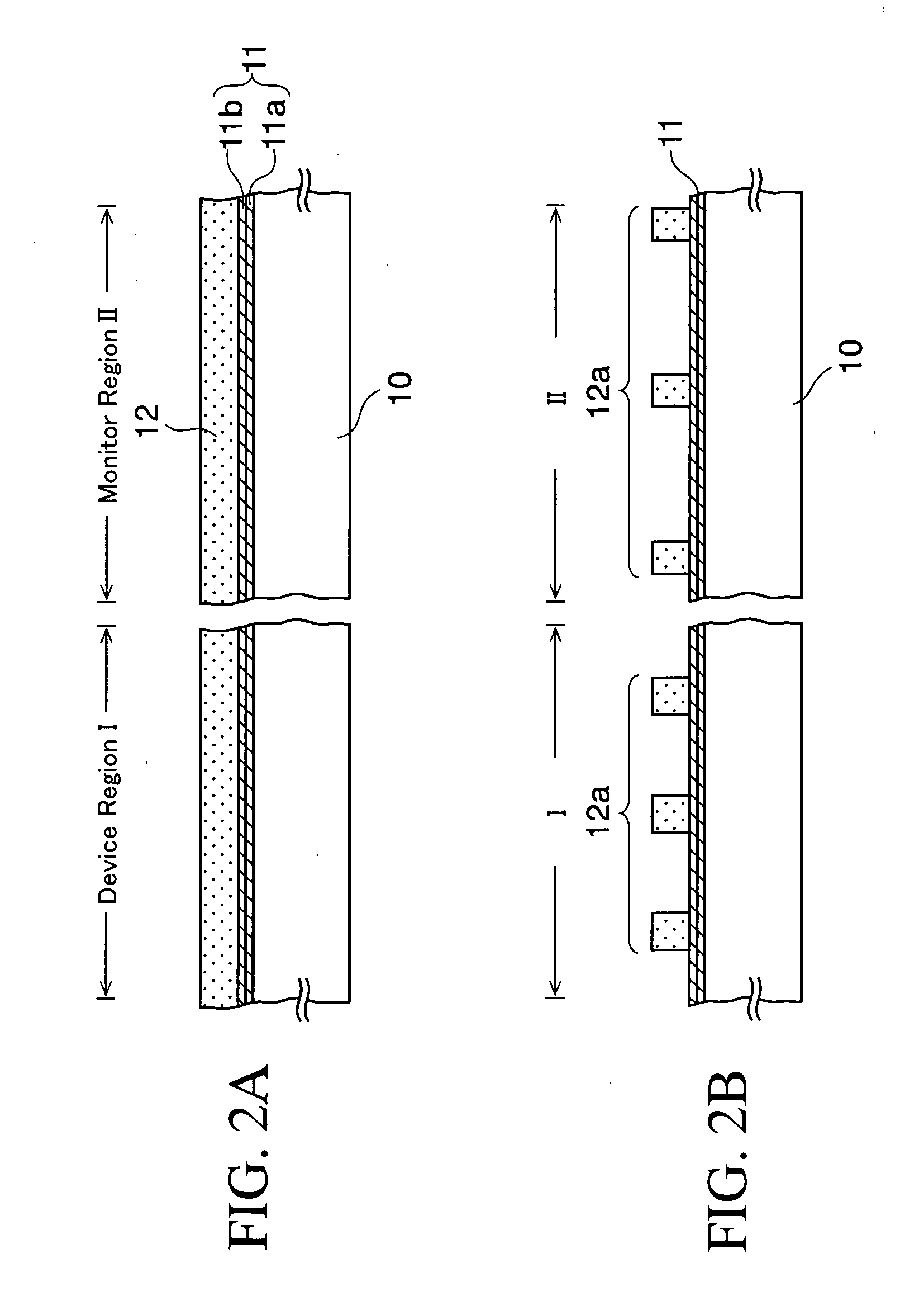
[0038] A quartz substrate (transparent substrate) 10, which has device region I where the light-shielding device patterns are formed and monitor region II where the phase difference of exposure light is measured, is brought into a sputtering chamber (not shown) first. The device region I is a region for obtaining an exposure pattern that is used when patterning metal wirings, gate electrodes, holes of an insulating film, or the like.
[0039] Further, although the size of the quartz substrate 10 is not particularly limited, a substrate having the side size of 6 inches and the thickness of 0.25 inch is employed in this embodiment. Then, with a sputtering method using Ar (argon) gas, a Cr (chromium) layer 11a is...
second embodiment
(2) Second Embodiment
[0084]FIGS. 6A to 6F are the in-process sectional views of the mask for exposure according to the second embodiment of the present invention. In these drawings, reference numerals same as those of the first embodiment are attached to elements explained in the first embodiment, and their explanation will be omitted in the following.
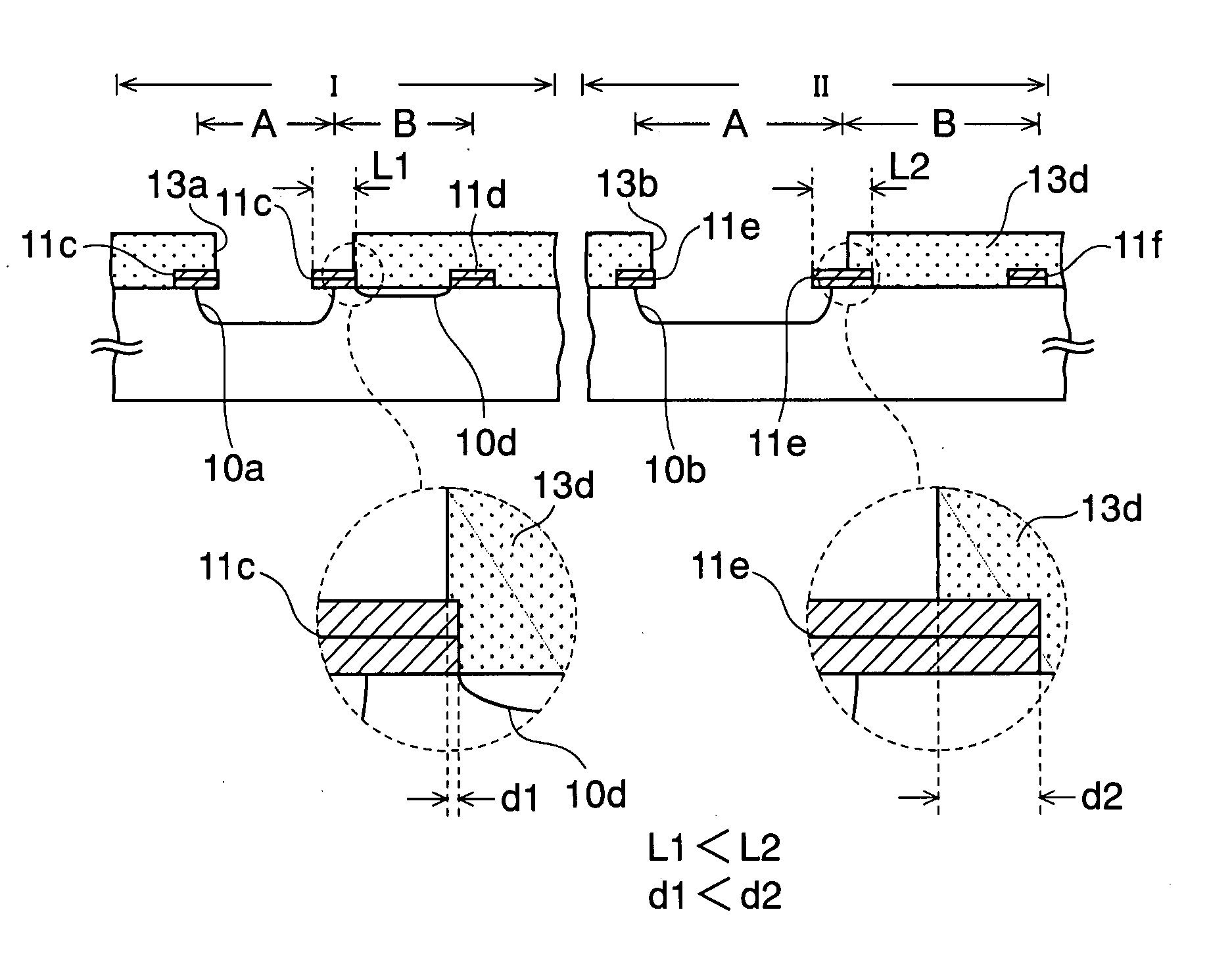
[0085] In the first embodiment, the size L2 of the first light-shielding monitor pattern lie in the monitor region II was set to equal to or less than the size L1 of the first light-shielding device pattern 11c in the device region I or less, and the phase difference of the device region I was guaranteed by the phase difference of the monitor region II.
[0086] On the contrary, in this embodiment, the overlap amount between the resist pattern and the light-shielding pattern is set as follows in order to obtain advantages same as the first embodiment.
[0087] Firstly, by performing the process of FIGS. 2A to 2D explained in the first emb...
third embodiment
(3) Third Embodiment
[0106] In the first embodiment described above, the size equal to or less than the size L1 of the first light-shielding device pattern 11c was employed as the size L2 of the first light-shielding monitor pattern 11e in the monitor region II, and when the erosion 10d of the quartz substrate 10 occurred in the non-shifter portion B of the device region I, the erosion 10d was allowed to occur in the non-shifter portion B of the device region I in the same manner. This could match the phase differences of the monitor region II and the device region I, and the phase difference of the monitor region II could guarantee the phase difference of the device region I.
[0107] However, if the phase difference of the monitor region II is actually shifted from 180 degrees, it is hard to determine whether such shift was caused by too much or too little etching to the second concave portion 10b or caused by the erosion 10d of the quartz substrate 10 in each region (I, II).
[0108] ...
PUM
| Property | Measurement | Unit |
|---|---|---|
| size | aaaaa | aaaaa |
| thickness | aaaaa | aaaaa |
| size | aaaaa | aaaaa |
Abstract
Description
Claims
Application Information