Production method for thin-film crystal wafer, semiconductor device using it and production method therefor

a production method and technology of thin-film crystals, applied in the direction of crystal growth process, polycrystalline material growth, chemically reactive gases, etc., can solve the problems of potential barrier formation, inhibiting smooth flow of current, and forming of potential barrier, so as to prevent unnecessary potential barrier formation, improve chemical stability, and suppress the formation of surface defects level

Inactive Publication Date: 2006-03-23
SUMITOMO CHEM CO LTD
View PDF6 Cites 9 Cited by
  • Summary
  • Abstract
  • Description
  • Claims
  • Application Information

AI Technical Summary

Benefits of technology

[0031] By forming a Si-layer on a III-V group compound semiconductor single crystal epitaxial layer, it is possible to suppress the formation of a surface defect level on the surface of the III-V group compound semiconductor single crystal epitaxial layer and to effectively prevent an ...

Problems solved by technology

In other words, formation of electrodes that can obtain ohmic connection capable of efficiently flowing current between the same and external devices has become an important technical problem.
However, even when the electrode material to be mounted on a semiconductor crystal is selected from the viewpoint as described above, there is a problem that instability at the surface of the semiconductor crystal causes a potential barrier to form, and that the barrier inhibits a smooth flow of current.
Therefore, the depletion layer makes it practically difficult to obtain ideal ohmic properties even if an el...

Method used


Image

  • Production method for thin-film crystal wafer, semiconductor device using it and production method therefor
  • Production method for thin-film crystal wafer, semiconductor device using it and production method therefor

Examples


Embodiment Construction

[0033] An exemplary embodiment of the present invention will now be described in detail with reference to the drawing.

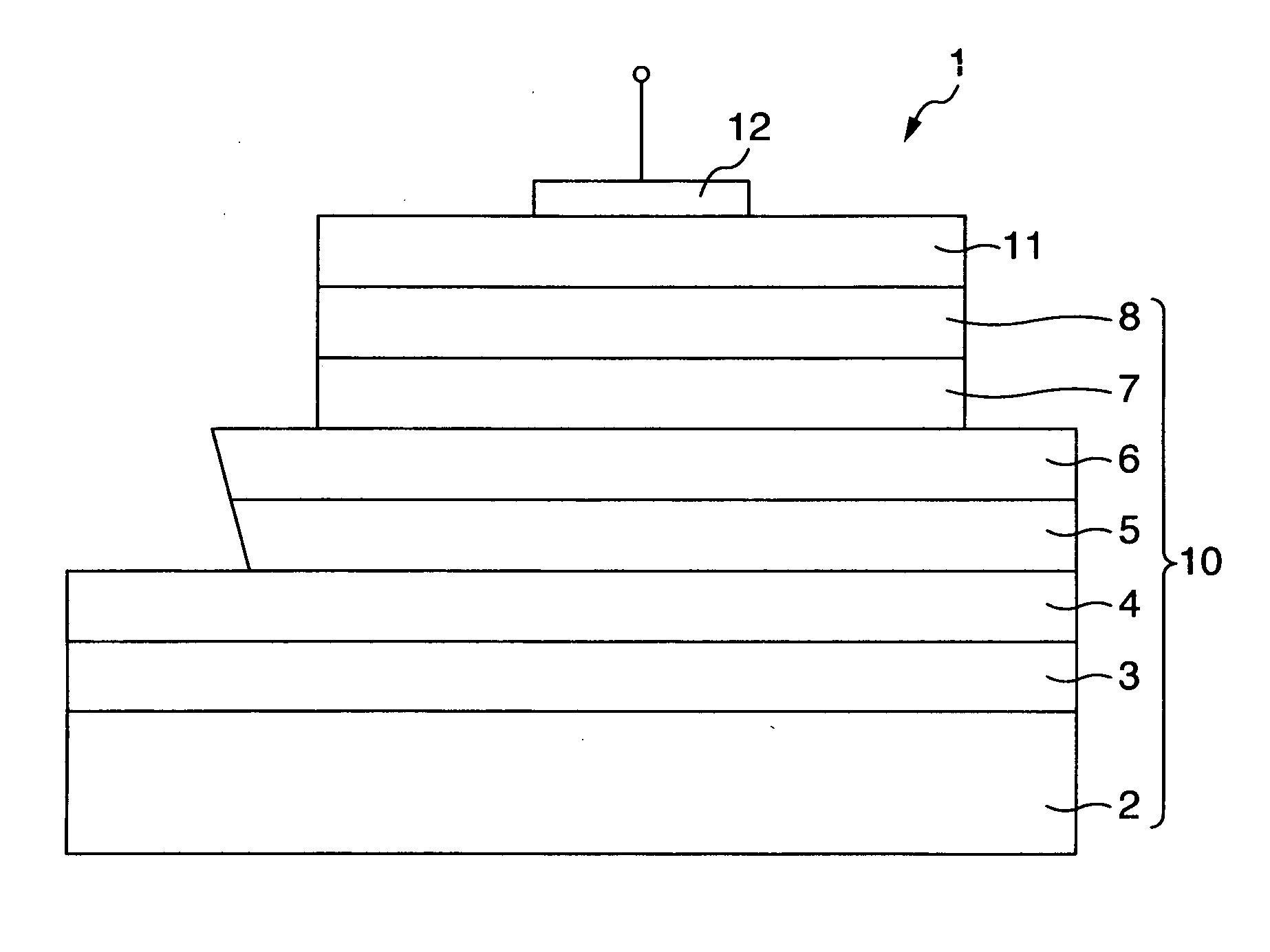
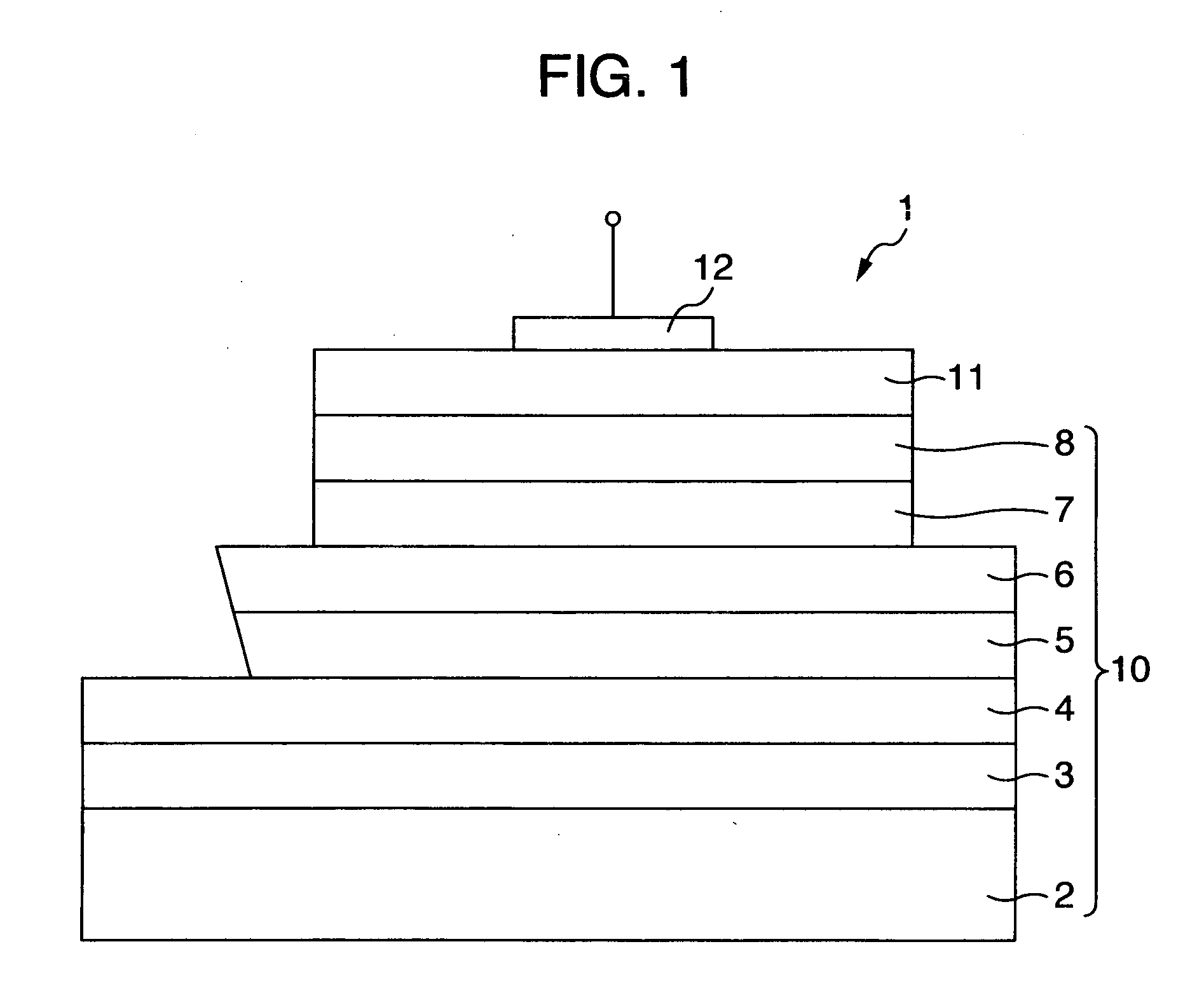
[0034]FIG. 1 shows an exemplary embodiment of a semiconductor device according to the present invention in a sectional view. The semiconductor device shown in FIG. 1 is a hetero-junction bipolar transistor (HBT) 1 that is built using a III-V group compound semiconductor crystal. HBT 1 is built using a GaAs single crystal 10, which is a III-V group compound semiconductor single crystal for HBT having a known configuration, and by which it functions as an HBT device. The GaAs single crystal 10 is manufactured by successively laminating, on a GaAs substrate 2, a buffer layer 3, an n+-GaAs layer (conductive layer) 4, an n-GaAs layer (collector layer) 5, a p-GaAs layer (base layer) 6, an n-InGaP layer (emitter layer) 7, an n+-GaAs layer (emitter cap layer) 8, in an appropriate epitaxial growth furnace, by an appropriate epitaxial growth method such as a metal organic vap...


PUM


Abstract

The n+-GaAs layer 8 of the GaAs single crystal 10 is formed by epitaxial growth, followed by epitaxially growing the Si-layer 11 in the same epitaxial growth furnace, and then the aluminum electrode 12 is formed on the Si-layer 11 as an ohmic electrode. The Si-layer 11 can suppress the formation of a surface defect level on the surface of the n+-GaAs layer 8 and can effectively prevent the formation of an unnecessary potential barrier. Since the Si-layer 11 has a smooth surface and is excellent in chemical stability, a good ohmic electrode can be obtained by forming the electrode 12 using aluminum or the like has a suitable work function to the Si-layer 11.

Description

TECHNICAL FIELD [0001] The present invention relates to a method for producing semiconductor wafers excellent in surface stability, and to semiconductor devices with good ohmic electrode properties using the same and a method for producing the semiconductor devices. BACKGROUND ART [0002] III-V group compound semiconductor crystals such as GaAs, GaP and GaN are widely used for the production of semiconductor devices such as high-speed electron devices used in a high-frequency region of microwave bands or higher, or light-emitting devices such as various light-emitting diodes. When the compound semiconductor crystals as described above are used to produce semiconductor devices, electrical properties of the semiconductor crystal itself is naturally important. However, from the viewpoint of device applications, electrical properties of the electrode part for electrically connecting the semiconductor crystal to external devices are also important. In other words, formation of electrodes ...

Claims


Application Information

Patent Timeline
IPC IPC(8): C30B23/00C30B25/00C30B28/12C30B28/14H01L21/28H01L21/203H01L21/205H01L21/285H01L21/331H01L29/267H01L29/417H01L29/45H01L29/737H01L33/30H01L33/36
CPCH01L21/28575H01L29/456H01L29/267
Inventor HATA, MASAHIKO
Owner SUMITOMO CHEM CO LTD
Why Eureka
Try Eureka