

RF grounding of cathode in process chamber
a cathode and process chamber technology, applied in the direction of coating, coating, chemical vapor deposition coating, etc., can solve the problems of less system effectiveness, time-consuming, difficult chamber cleaning,
- Summary
- Abstract
- Description
- Claims
- Application Information
AI Technical Summary
Benefits of technology
Problems solved by technology
Method used
Image

Examples
Embodiment Construction
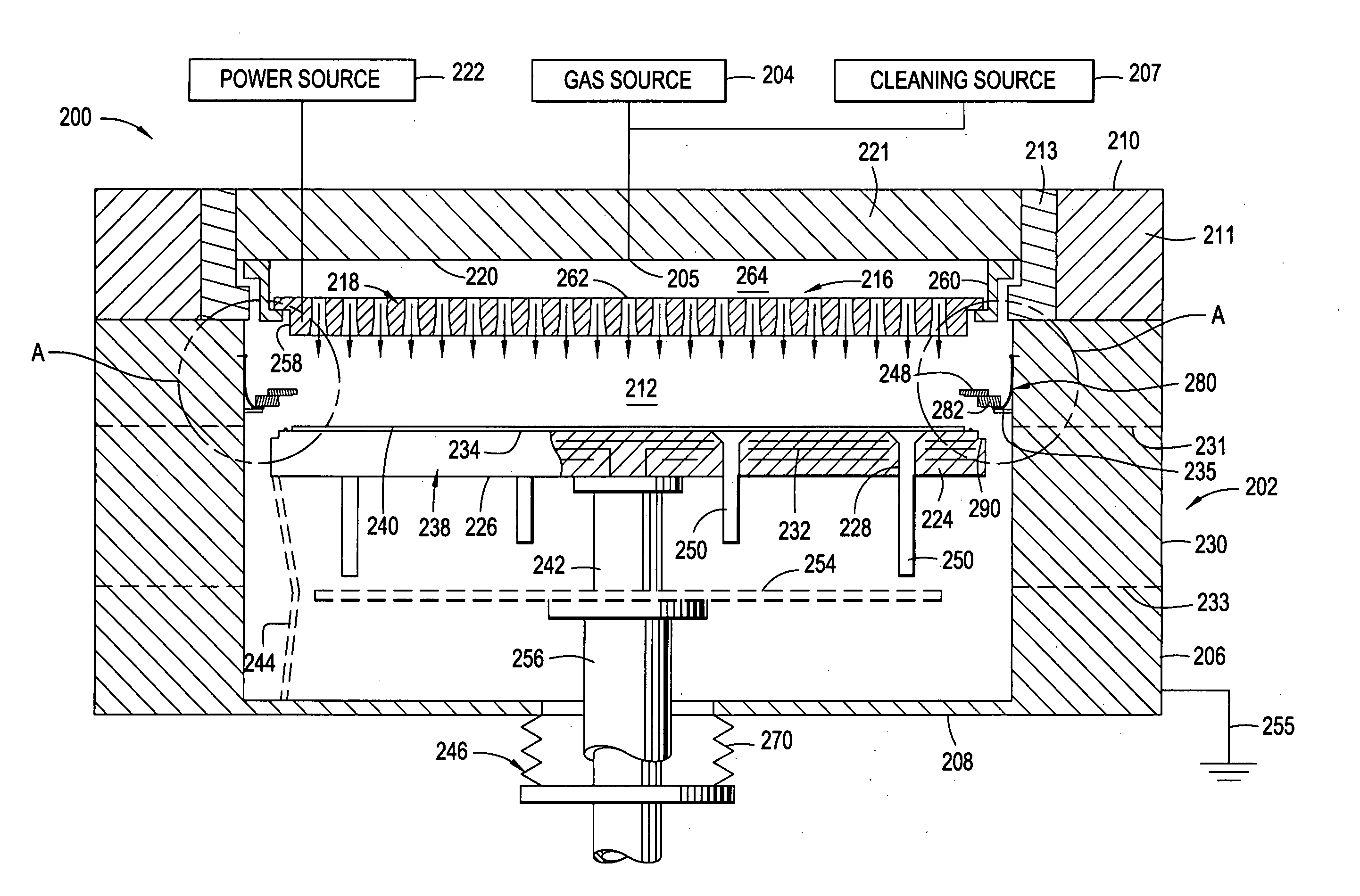
[0030] The invention generally provides an RF current return path for systems supporting large area substrates. The invention is illustratively described below in reference to a plasma enhanced chemical vapor deposition (PECVD) system, such as those commercially available from AKT, a division of Applied Materials, Inc. of Santa Clara, Calif. However, it should be understood that the invention has utility in other system configurations such as physical vapor deposition systems, etch systems and other processing systems in which a low-impedance RF current return path between a substrate support and a chamber housing the substrate support is desired.
[0031] Embodiments of the invention create better ways to uniformly RF ground the susceptor in an RF plasma chamber. Typically, process chambers are not completely symmetrical in terms of structures. For example, one side of the chamber might have a port in the chamber wall for transferring substrates in and out of the process chamber. The...
PUM
| Property | Measurement | Unit |
|---|---|---|
| Length | aaaaa | aaaaa |
| Length | aaaaa | aaaaa |
| Length | aaaaa | aaaaa |
Abstract
Description
Claims
Application Information