Solid state image pickup device and method for manufacturing the same

a solid-state image and pickup device technology, applied in the direction of diodes, semiconductor devices, radiation-controlled devices, etc., can solve the problems of impurity atoms, implantation damage, and change in the well potential of p-wells

Active Publication Date: 2006-03-23
SONY CORP
View PDF4 Cites 22 Cited by
  • Summary
  • Abstract
  • Description
  • Claims
  • Application Information

AI Technical Summary

Problems solved by technology

For example, if a drain voltage changes while power is being supplied by a whole-surface drain wiring, coupling between the whole-surface drain wiring and the p-well occurs, which leads to a change in a well potential of the p-well.
However, such high-concentration ion implantation often causes implantation damage (e.g., crystal defect) or mixing of impurity atoms, such as an undesired heavy metal.
If a high-concentration p-type doped region is adjacent to the photodiode, a dark current occurs due to an intense electric field between the p-type doped region and an n-type layer of the photodiode, which may be a cause of white spots.
These white spots result in degradation in an image quality, which arises a problem.
A problem to be solved is that, when a large amount of impurity need be introduced by an ion implantation technique or the like in order to provide a contact in a pixel, a dark current occurs due to an incidental crystal defect and mixing of an undesired impurity, which causes white spots.

Method used


Image

  • Solid state image pickup device and method for manufacturing the same
  • Solid state image pickup device and method for manufacturing the same
  • Solid state image pickup device and method for manufacturing the same

Examples


first embodiment

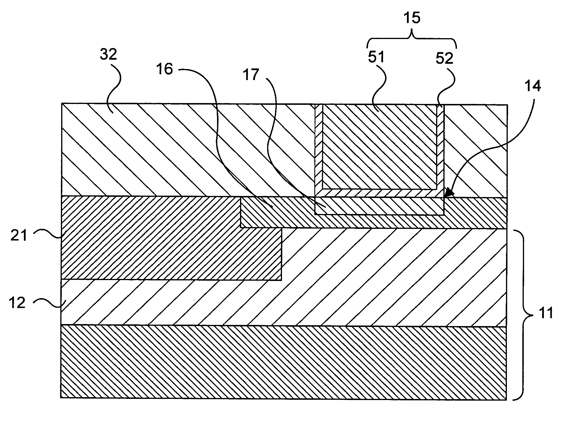
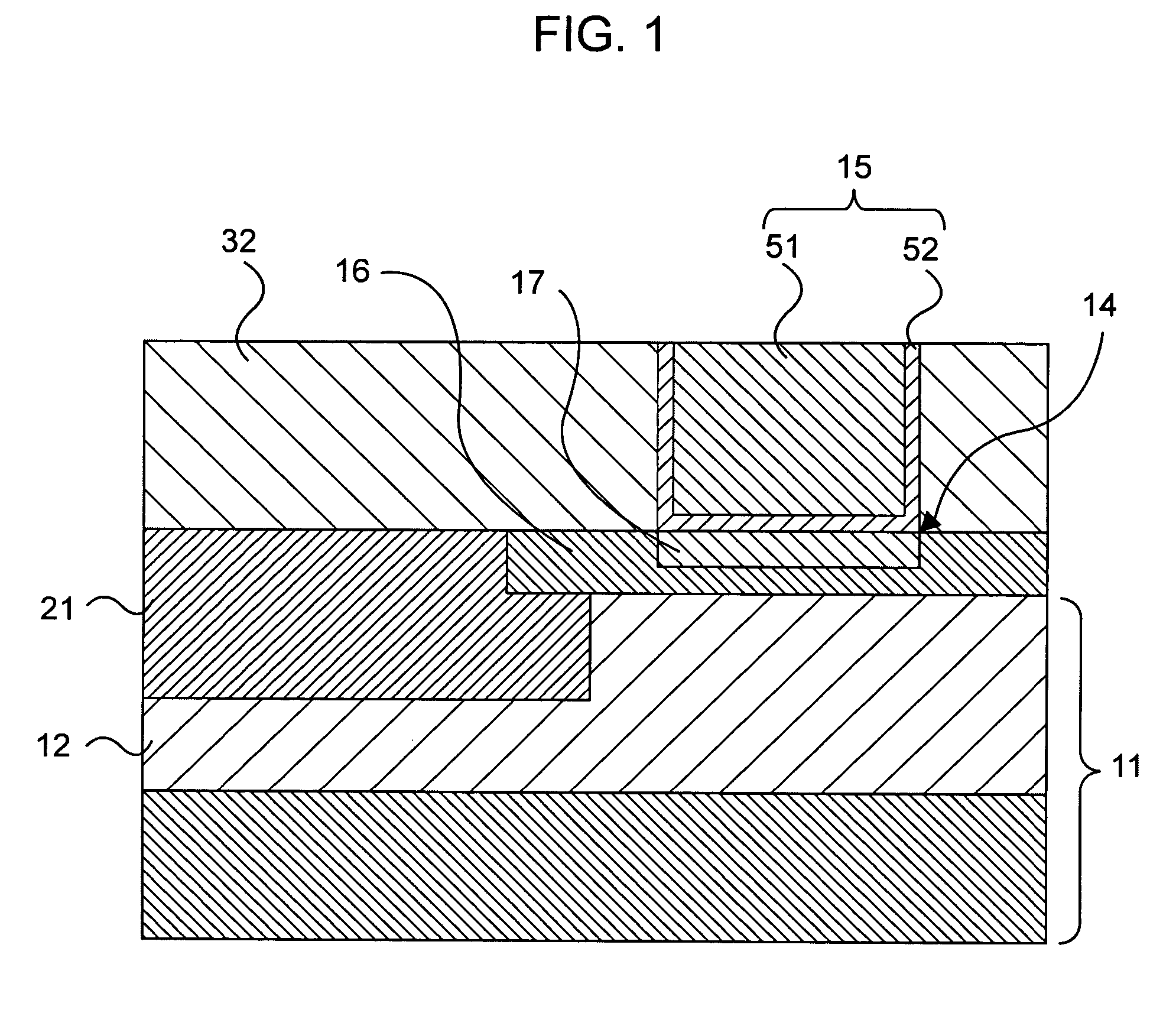
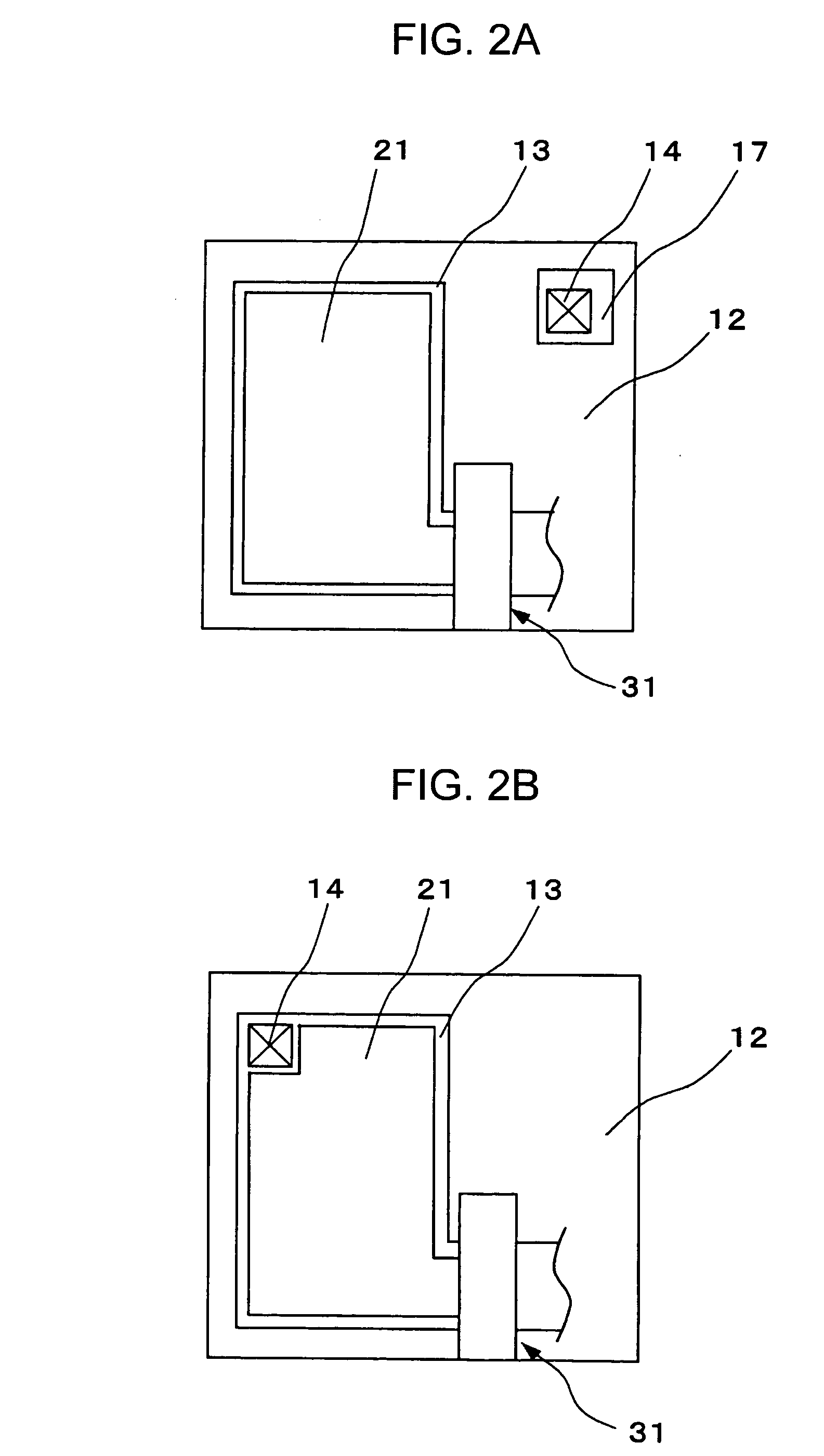
[0028] Hereinafter, a solid state image pickup device and a method for manufacturing the same according to the present invention will be described with reference to FIG. 1, which is a cross-sectional view showing a schematic configuration, and FIGS. 2A and 2B, which show plane layouts. In FIGS. 1, 2A, and 2B, a main portion of one pixel according to the invention is shown. In the following description, a first conductive type is a p-type and a second conductive type is an n-type.

[0029] As shown in FIGS. 1, 2A, and 2B, a semiconductor substrate 11 includes a pixel region provided with a plurality of pixels, each pixel including a photoelectric converter 21 and a transfer transistor 31 (not shown in FIG. 1); and a pixel well 12 shared by the respective pixels. The photoelectric converter 21 includes a photodiode or the like and the transfer transistor 31 includes an n-channel MOS transistor or the like. The photoelectric converter 21 is an n-type region, is used for conducting photoel...

second embodiment

[0043] Next, a solid state image pickup device and a method for manufacturing the same according to the present invention will be described with reference to FIG. 6, which is a cross-sectional view showing a schematic configuration. In FIG. 6, a main portion of one pixel according to the invention is shown.

[0044] As shown in FIG. 6, a semiconductor substrate 11 includes a pixel region provided with a plurality of pixels, each pixel including a photoelectric converter 21 and a transfer transistor (not shown); and a pixel well 12 shared by the respective pixels. The photoelectric converter 21 includes a photodiode or the like and the transfer transistor includes an n-channel MOS transistor or the like. The photoelectric converter 21 is an n-type region, is used for conducting photoelectric conversion, and serves as a signal charge accumulating portion.

[0045] The pixel well 12 is provided with a well contact 14 supplying a reference voltage for stabilizing a well potential. The well c...


PUM


Abstract

To reduce white spots by optimizing an impurity concentration of a p-type impurity doped region of a well contact, a size of a contact portion, a position of an n-type region serving as a photoelectric converter, and so on. In a solid state image pickup device in which a semiconductor substrate 11 includes a pixel region where a plurality of pixels are arranged, each pixel including a photoelectric converter 21, and a pixel well 12 shared by the respective pixels, a well contact 14 supplying a reference voltage to the pixel well 12 includes: an electrode 15 supplying a reference voltage; a p-type impurity doped region 16 placed in a surface of the pixel well 12; and a contact portion 17 placed in the p-type impurity doped region 16 so as to be connected to the electrode 15 and having a higher concentration than the p-type impurity doped region 16. The p-type impurity doped region 16 is doped with at least a p-type impurity, with an impurity concentration of 1×1019 cm−3 or less.

Description

CROSS PREFERENCE TO RELATED APPLICATIONS [0001] The present invention claims the benefit of Japanese Patent Application JP 2004-252262 filed in the Japanese Patent Office on Aug. 31, 2004, the entire contents of which are incorporated herein by reference. FIELD OF THE INVENTION [0002] The present invention relates to a solid state image pickup device and a method for manufacturing the same for easily reducing defects white spots in the dark. BACKGROUND OF THE INVENTION [0003] In a solid state image pickup device, particularly in a CMOS (complementary metal oxide semiconductor) sensor, when many pixels are arranged in an array pattern (hereinafter, a region where many pixels are arranged in an array pattern is called a “pixel region”) and when a well potential of a common p-well is applied thereto from immediately outside a periphery of the pixel region, that is, from immediately outside a most external pixel, a time constant is different in a peripheral portion of the pixel region n...

Claims


Application Information

Patent Timeline
Patent Type & Authority Applications(United States)
IPC IPC(8): H01L29/04
CPCH01L27/14609H01L27/14689H01L27/14643H01L27/146
Inventor WAKANO, TOSHIFUMIMABUCHI, KEIJINAKASHIKIRYO, TAKASHIMATSUBAYASHI, KAZUNARI
Owner SONY CORP
Why Eureka
Try Eureka