
Semiconductor device and semiconductor device unit

a semiconductor device and semiconductor technology, applied in semiconductor devices, semiconductor/solid-state device details, electrical apparatus, etc., can solve the problems of increasing and reducing the impedance between the external addition circuit and the first corner lead. , to achieve the effect of preventing the increase of the size of the semiconductor device unit and reducing the impedan

Inactive Publication Date: 2006-03-23
SOCIONEXT INC
View PDF4 Cites 1 Cited by
  • Summary
  • Abstract
  • Description
  • Claims
  • Application Information

AI Technical Summary

Benefits of technology

[0017] Another object of the present invention is to provide a semiconductor device and semiconductor device unit which can attain high-density arrangement of the leads and the miniaturization of the device.
[0035] As described above, according to the present invention, the vertex portions of the stage which are the four-corner positions of the stage are effectively used for the arrangement of the leads, and it is possible to attain high-density arrangement of the leads as well as the miniaturization of the semiconductor device.

Problems solved by technology

However, in the conventional semiconductor devices mentioned above, the outwardly extended portions extending along the diagonal line linking two of the four corners of the semiconductor supporting lead frame as in Japanese Laid-Open Patent Applications No. 09-293822, and the outwardly extended portions which extend from the four corners of the metal tab as in Japanese Laid-Open Patent Applications No. 07-030067 are cut away after formation of the package and they do not serve as the external connection terminals.
Therefore, in the conventional semiconductor devices, the entire circumference of the package is not effectively used for the arrangement of the leads, and there is the problem that the size of the semiconductor device is increased.
Hence, the width of the leads connected to the power supply and the ground also becomes narrow.
However, it is difficult for the conventional semiconductor devices to attain low impedance of the leads connected to the power supply and the ground, and there is the problem that the electrical properties deteriorate.

Method used


Image

  • Semiconductor device and semiconductor device unit
  • Semiconductor device and semiconductor device unit
  • Semiconductor device and semiconductor device unit

Examples


Embodiment Construction

[0045] A description will now be given of the preferred embodiments of the present invention with reference to the accompanying drawings.

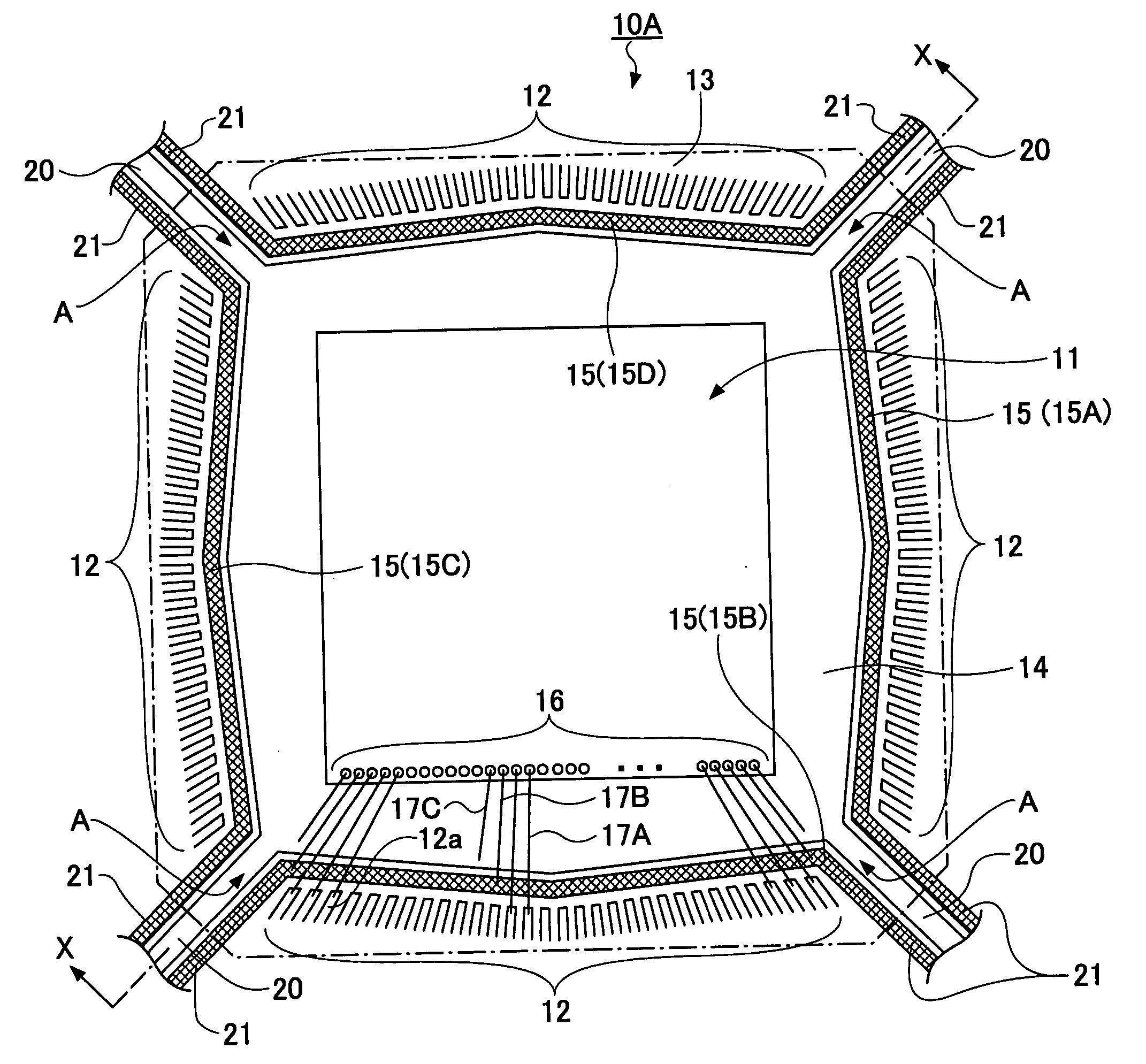
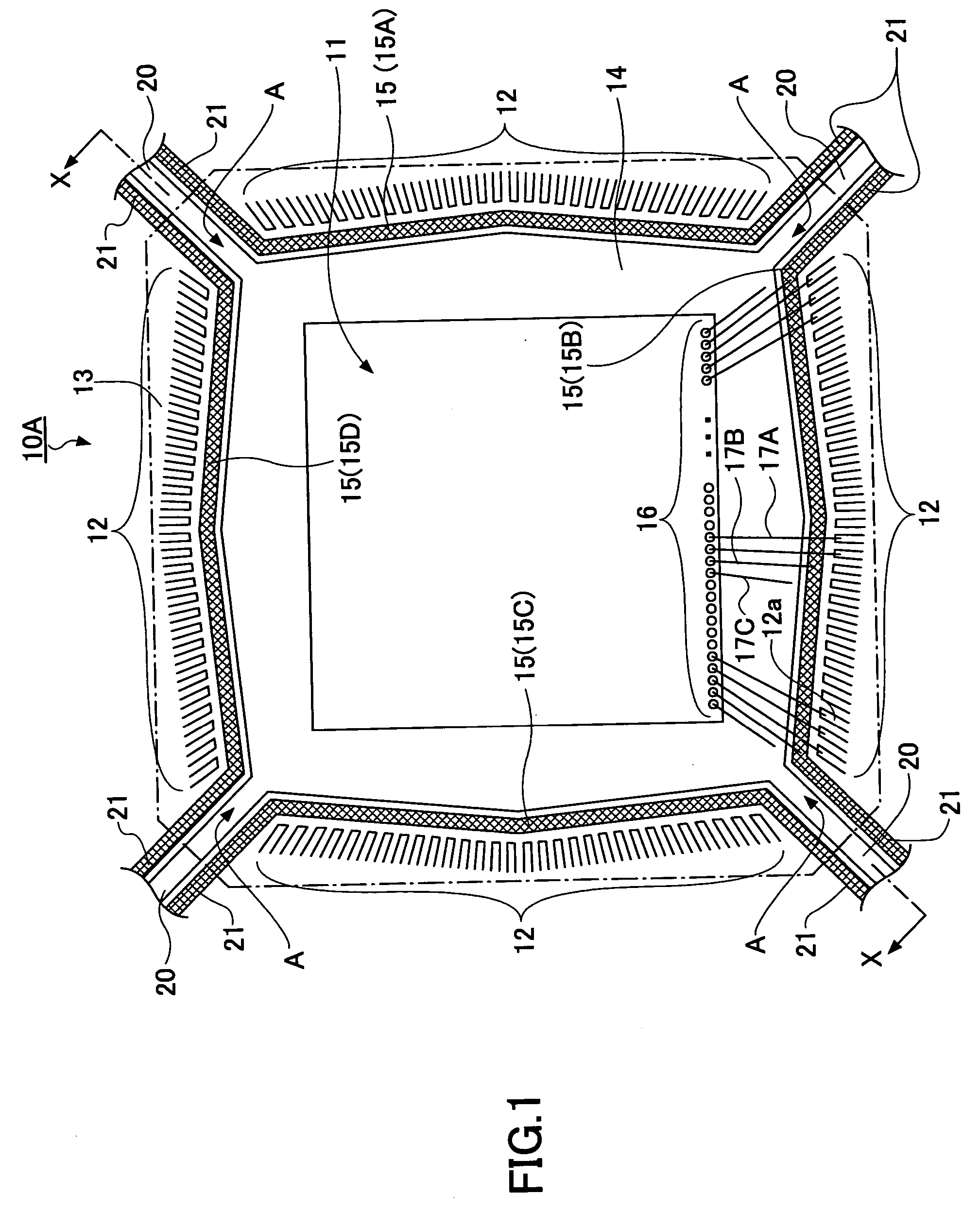
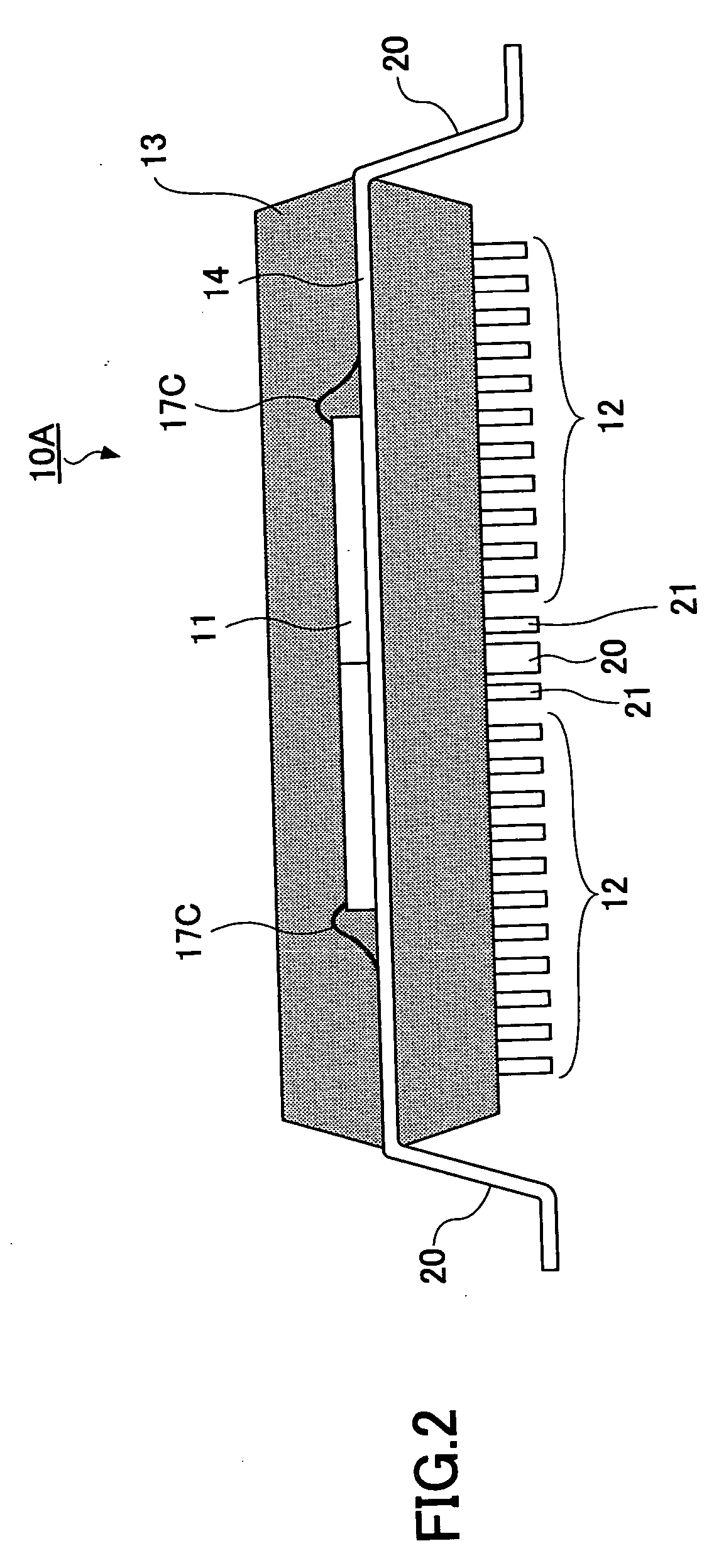
[0046] With reference to FIG. 1 through FIG. 3, the composition of the semiconductor device 10A in the first preferred embodiment of the invention will be explained.

[0047]FIG. 1 shows the principal part of the semiconductor device 10A in the state where the resin package 13 is considered transparent, FIG. 2 is a cross-sectional view of the semiconductor device 10A taken along the line X-X in FIG. 1, and FIG. 3 is a diagram for explaining the arrangement of the leads at the vertex portions of the semiconductor device 10A. The arrangement of the leads will be explained later.

[0048] The semiconductor device 10A has the QFP (Quad Flat Package) structure, and the semiconductor device 10A generally comprises the semiconductor chip 11, the leads 12, the resin package 13, the stage 14, and the outer peripheral leads 15.

[0049] The semiconductor chip 11 ...


PUM


Abstract

A semiconductor device comprises a semiconductor chip which is mounted on a stage. A plurality of leads are electrically connected with the semiconductor chip. A package encloses the semiconductor chip and a part of the plurality of leads. A first corner lead is provided in the stage and outwardly extends from at least one of vertex portions at four corners of the stage to an exterior of the package.

Description

CROSS-REFERENCE TO RELATED APPLICATIONS [0001] This application is based upon and claims the benefit of priority of Japanese Patent Application No. 2004-271910, filed on Sep. 17, 2004, the entire contents of which are herein incorporated by reference. BACKGROUND OF THE INVENTION [0002] 1. Field of the Invention [0003] The present invention generally relates to a semiconductor device and semiconductor device unit, and more particularly to a semiconductor device and semiconductor device unit which can provide high-density arrangement. [0004] 2. Description of the Related Art [0005] In recent years, the semiconductor device with advanced functions and multiple bit features has been rapidly proliferated, and, in connection with this, the number of the leads tends to be increased. [0006] On the other hand, the miniaturization of the semiconductor device is demanded, and it is necessary to adopt the smaller pitch of the leads. Therefore, it is desirable to provide the semiconductor device...

Claims


Application Information

Patent Timeline
Patent Type & Authority Applications(United States)
IPC IPC(8): H01L23/495
CPCH01L23/49503H01L23/49537H01L2224/48253H01L2924/014H01L2924/01033H01L2924/01006H01L23/49541H01L23/49589H01L24/49H01L2224/48091H01L2224/48247H01L2224/49171H01L2924/01004H01L2924/01029H01L2924/01082H01L2924/19041H01L2924/30105H01L2924/3011H01L24/48H01L2224/48257H01L2924/00014H01L2924/00H01L2224/05554H01L2924/15787H01L2224/45099H01L2224/05599
Inventor ISE, HISAO
Owner SOCIONEXT INC
Learn More