Semiconductor device having a switch circuit

a switch circuit and semiconductor technology, applied in the field of semiconductor devices, can solve the problems of further minimization of the size of the leads, difficult for the semiconductor device to be miniaturized by the further minimization of the lead size, etc., and achieve the effect of reducing the number of power source leads and facilitating miniaturization of the semiconductor devi

Inactive Publication Date: 2006-03-23
RENESAS ELECTRONICS CORP
View PDF5 Cites 7 Cited by
  • Summary
  • Abstract
  • Description
  • Claims
  • Application Information

AI Technical Summary

Benefits of technology

[0007] The number of bonding pads of a semiconductor chip is steadily increasing along with the demand for higher packaging and multi-functioning of the integrated circuits which are mounted on the semiconductor chip. The number of leads increases along with an increase in the number of bonding pads, and, hence, the profile size of the semiconductor device has increased. Accordingly, efforts have been made to miniaturize the semiconductor device by narrowing the arrangement pitch of leads by minimizing the size of the leads. With respect to a recent QFP type semiconductor device, the arrangement pitch gas been narrowed to a level of 0.3[mm] to 0.4[mm]. However, a given bonding area is necessary to ensure reliability at the time of mounting the semiconductor device on a printed wiring circuit board by soldering, and a sufficient mechanical strength is necessary to some extent to suppress bending of the leads. Accordingly, it is considered that further miniaturization of the semiconductor device by the further minimization of size of the leads is difficult.
[0009] It is an object of the present invention to provide a technique which can miniaturize a semiconductor device.
[0014] According to the abovementioned example, it is possible to reduce the number of power source leads which are electrically connected to second power source leads via the bonding wires and, hence, the semiconductor device can be miniaturized.

Problems solved by technology

Accordingly, it is considered that further miniaturization of the semiconductor device by the further minimization of size of the leads is difficult.

Method used


Image

  • Semiconductor device having a switch circuit
  • Semiconductor device having a switch circuit
  • Semiconductor device having a switch circuit

Examples


embodiment 1

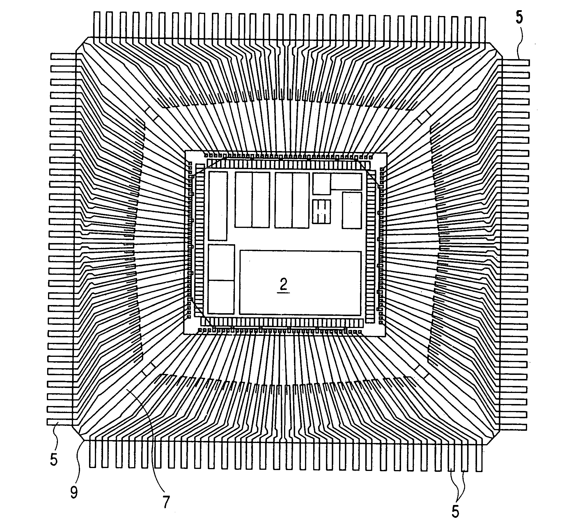
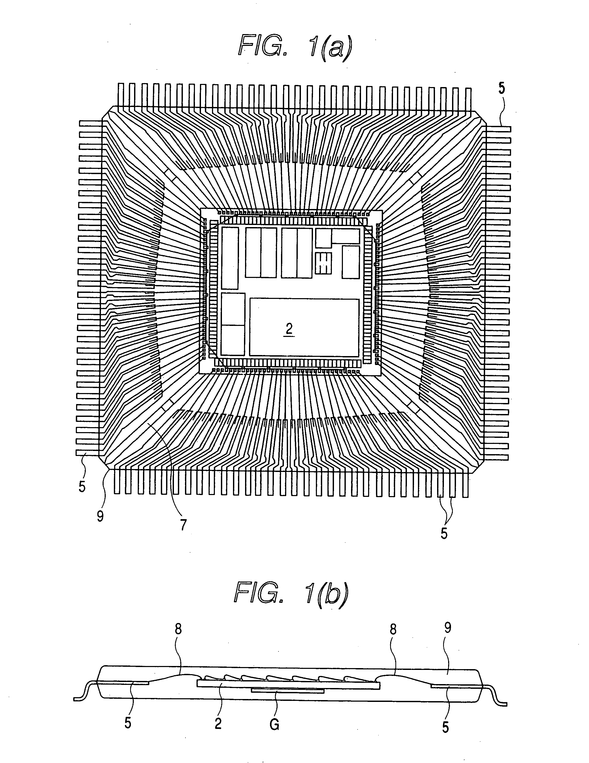
[0060] In this embodiment 1, an explanation will be directed to an example in which the present invention is applied to a QFP (Quad Flatpack Package) type semiconductor device with reference to FIGS. 1(a) to 11.

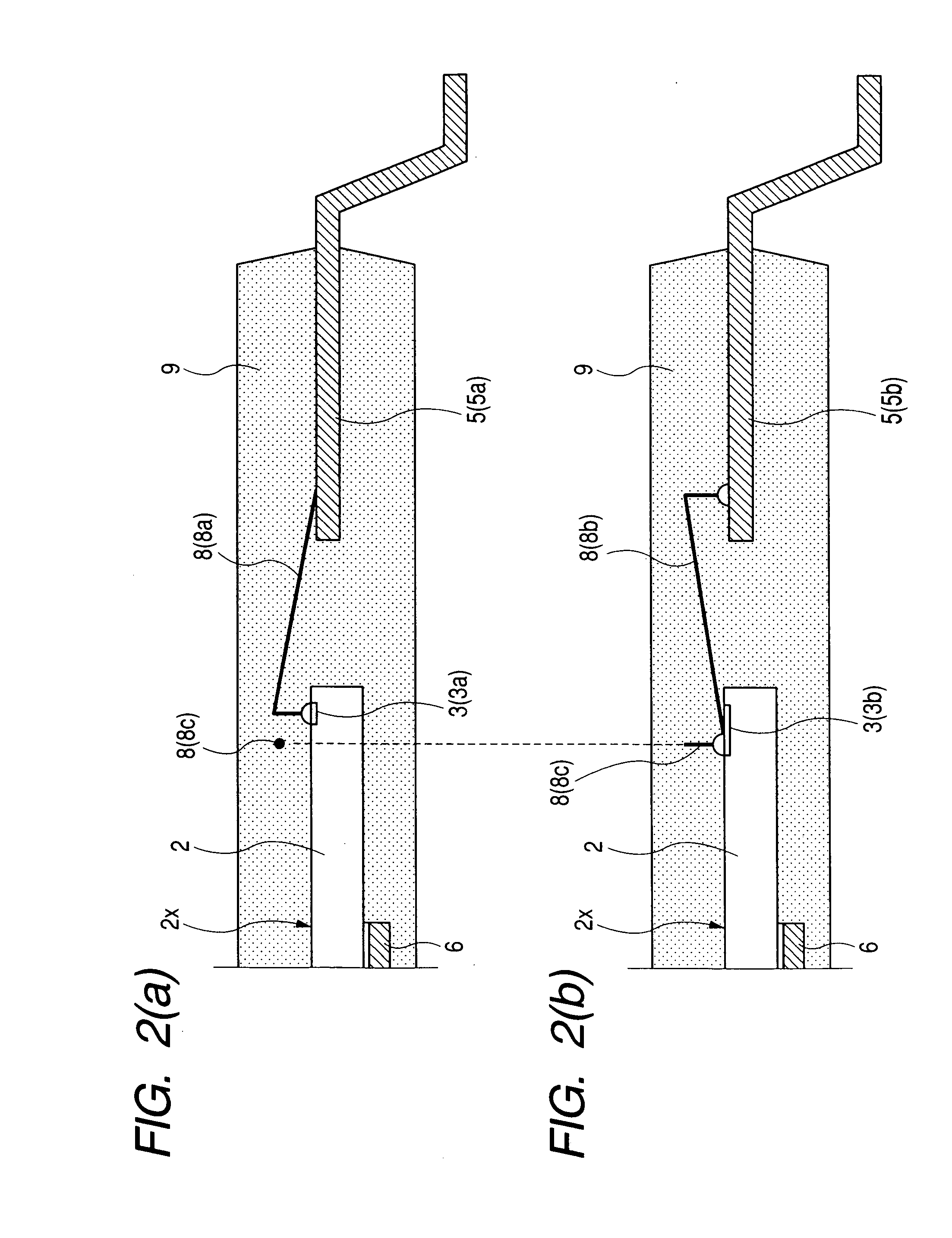
[0061] As shown in FIG. 1(a) to FIG. 3, the semiconductor device of this embodiment 1 is mainly constituted of a semiconductor chip 2, a plurality of leads 5, a plurality of bonding wires 8, a sealing body 9 and the like. The semiconductor chip 2 is fixed by adhesion to a support body 6, which is referred to as a tab or a die pad, while, for example, four suspension leads 7 are integrally connected to the support body 6.

[0062] As shown in FIG. 7, the planar shape of the semiconductor chip 2 along the thickness direction thereof is formed in a quadrangular shape. In this embodiment 1, for example, the planar shape of the semiconductor chip 2 is formed in a square shape having a size of 7.6[mm]×7.6[mm].

[0063] Although the semiconductor chip 2 is not limited to the following ...

embodiment 2

[0107] In connection with the abovementioned embodiment 1, the explanation was directed to the example in which the number of the power source leads is reduced using the bonding wires. In this embodiment 2, an explanation will be directed to an example in which the number of the power source leads is reduced using relay bonding pads and bonding wires, with reference to FIGS. 15(a) to 22.

[0108] As shown in FIG. 21, a plurality of buffer cells 4 include a plurality of power source cells 4b2 and a plurality of bonding pads 3 include a plurality of power source bonding pads 3b2. The plurality of power source cells 4b2 are arranged at locations corresponding to the plurality of power source bonding pads 3b2.

[0109] Although not shown in the drawing, on an internal circuit forming portion 10, a power source line which supplies an operational potential (for example, 0V=Vss) to a plurality of input / output cells 4a, for example, is arranged. This power source line extends in a ring-like sha...

embodiment 3

[0119] This embodiment 3 is directed to an example in which the number of leads is reduced by the combination of the abovementioned embodiments 1 and 2.

[0120]FIG. 23(a) and FIG. 23(b) show the inner structure of a semiconductor device according to an embodiment 3 of the present invention, wherein FIG. 23(a) is a plan view and FIG. 23(b) is a cross-sectional view;

[0121] As shown, the wire connection between bonding pads to which an operational potential (power source potential) Vcc is applied is established using the abovementioned embodiment 1 and the wire connection between bonding pads to which an operational potential (power source potential) Vss is applied is established using the abovementioned embodiment 2. In this manner, due to the combination of the abovementioned embodiments 1 and 2, the number of power source leads of two systems can be reduced, and, hence, it is possible to realize further miniaturization of the semiconductor device.


PUM


Abstract

A semiconductor device includes a semiconductor chip, a plurality of bonding pads which are formed on a main surface of the semiconductor chip and include first power source bonding pads, second power source bonding pads and a plurality of signal bonding pads, a plurality of leads which are arranged around the semiconductor chip and include first power source leads and a plurality of signal leads, a plurality of bonding wires which include first bonding wires for connecting the first power source bonding pads with the first power source leads, second bonding wires for connecting the first bonding pads with second bonding pads and third bonding wires for connecting the plurality of signal bonding pads with the plurality of signal leads, and a sealing body which seals the semiconductor chip, the plurality of bonding wires and some of the plurality of leads.

Description

CROSS-REFERENCE TO RELATED APPLICATION [0001] This application is a Continuation of application Ser. No. 10 / 860,072, filed Jun. 4, 2004, the entire disclosure of which is hereby incorporated by reference.BACKGROUND OF THE INVENTION [0002] The present invention relates to a semiconductor device, and, more particularly, to a technique which is effectively applicable to a semiconductor device in which bonding pads of a semiconductor chip are connected to connecting portions which are arranged around the semiconductor chip using bonding wires. [0003] Semiconductor devices having various package structures, which differ depending on the functions and kinds of integrated circuits mounted on a semiconductor chip, have been commercialized. As one example of these semiconductor devices, there is a semiconductor device which is referred to as a QFP (Quad Flatpack Package) type semiconductor device. The QFP type semiconductor device is mainly constituted of a semiconductor chip having a main s...

Claims


Application Information

Patent Timeline
Patent Type & Authority Applications(United States)
IPC IPC(8): H01L23/34H01L21/60H01L23/12H01L23/485H01L23/495H01L23/528H01L23/538
CPCH01L23/4952H01L23/5286H01L24/05H01L24/06H01L24/45H01L24/48H01L24/49H01L24/85H01L2224/04042H01L2224/05553H01L2224/05556H01L2224/05624H01L2224/45144H01L2224/48091H01L2224/4813H01L2224/48247H01L2224/48465H01L2224/48471H01L2224/4903H01L2224/49051H01L2224/4911H01L2224/49171H01L2224/49173H01L2224/73265H01L2224/85951H01L2924/01004H01L2924/01005H01L2924/01006H01L2924/01013H01L2924/01014H01L2924/01015H01L2924/01029H01L2924/01033H01L2924/0105H01L2924/01078H01L2924/01079H01L2924/01082H01L2924/014H01L2924/05042H01L2924/12044H01L2924/14H01L2924/15311H01L2924/19043H01L2924/30105H01L2224/32225H01L2224/32245H01L2924/00014H01L2924/01019H01L2924/01023H01L2224/45124H01L2224/48624H01L2224/48227H01L2224/48699H01L2224/48137H01L2224/05554H01L2924/1306H01L2224/02166H01L2224/78H01L2924/00012H01L2924/00H01L2224/45015H01L2224/45147H01L2224/48824H01L2224/48724H01L2924/181H01L2224/85203H01L2224/85205H01L24/73H01L2224/023H01L2924/0001H01L23/12H01L23/538H01L21/60
Inventor SHIMANUKI, YOSHIHIKOHASUNUMA, HISASHI
Owner RENESAS ELECTRONICS CORP
Why Eureka
Try Eureka