Apparatuses and methods for integrating opto-electric components into the optical pathways of routing substrates with precision optical coupling and compact electrical interconnection

a technology of opto-electronic components and optical pathways, applied in the direction of optics, optical light guides, instruments, etc., can solve the problems of complex optical communication systems with large number of opto-electronic devices and high degree of functionality, and use less effective opto-electronic devices, so as to reduce signal delay to devices, improve the accuracy of optical alignment, and improve the effect of integration

Inactive Publication Date: 2006-03-23
FUJITSU LTD
View PDF21 Cites 11 Cited by
  • Summary
  • Abstract
  • Description
  • Claims
  • Application Information

AI Technical Summary

Benefits of technology

[0006] Broadly stated, the present invention encompasses apparatuses and methods for enabling the fast and reliable integration of opto-electric components onto optical routing substrates in a manner that enables accurate alignment of optical signals to and from the opto-electric components, and short electrical interconnect paths to the components to reduce signal delays to the devices on the opto-electric components. For each opto-electric component, an attachment area is set out on the optical routing substrate. Located adjacent to the attachment area are one or more optical waveguides for coupling (i.e., transmitting and / or receiving) optical signals with the component to be placed over the attachment area. A plurality of conductive pads are located within the attachment area, and are for interconnecting with the opto-electric component by way of bodies of solder or conductive adhesive, or the like. Also located within the attachment area and interspersed between the conductive pads are a plurality of spacers (preferably at least three) that set a spacing distance between the attachment area and the opposing surface of the opto-electric component. The thickness of the spacers is greater than the thickness of the conductive pads and is selected so as to align the core layers of the waveguides with the core layers of the opto-electric component. The alignment significantly reduces the optical losses in coupling optical signals to and from the opto-electric components.

Problems solved by technology

The information-technology (IT) industry is already encountering the physical limits of current electrical components, interconnections and assembly technologies.
However, that would require building complex optical communication systems with large numbers of opto-electronic devices and high degrees of functionality.
Currently, some of the most effective opto-electronic devices are constructed on substrates that cannot be used to construct the entire optical system, either because of prohibitive costs, and / or because such substrates are not large enough to support the entire optical system.
As one work-around to this problem, some have used less effective opto-electronic devices because they could be readily incorporated on the substrates used for large-scale optical systems.
However, this approach has the disadvantage of being constrained to using less effective opto-electronic devices.
However, this approach is expensive, is prone to misalignment of the optical core layers, usually requires precision polishing of the mini-substrates (to reduce their thicknesses), and constrains the processing temperatures for making the optical system to the highest temperature that the finished mini-substrate can withstand.
Misalignment of optical components causes significant attenuation of the light signal.
The possibility of misalignment must be considered when designing an optical system, and this consideration usually constrains the size and / or functionality of the optical system.

Method used


Image

  • Apparatuses and methods for integrating opto-electric components into the optical pathways of routing substrates with precision optical coupling and compact electrical interconnection
  • Apparatuses and methods for integrating opto-electric components into the optical pathways of routing substrates with precision optical coupling and compact electrical interconnection
  • Apparatuses and methods for integrating opto-electric components into the optical pathways of routing substrates with precision optical coupling and compact electrical interconnection

Examples


Embodiment Construction

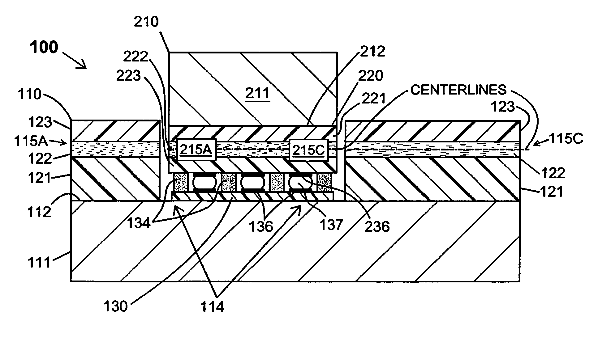
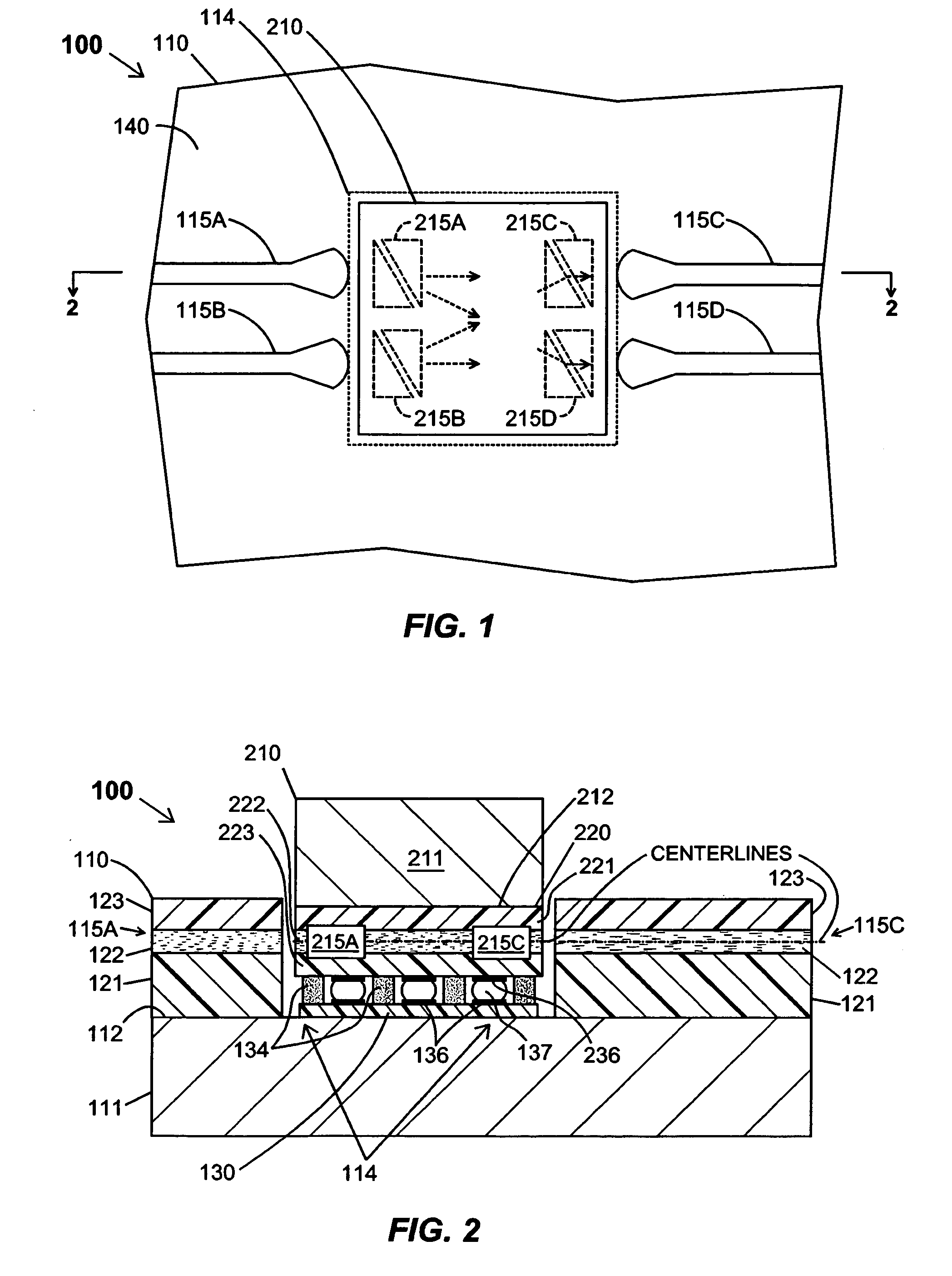
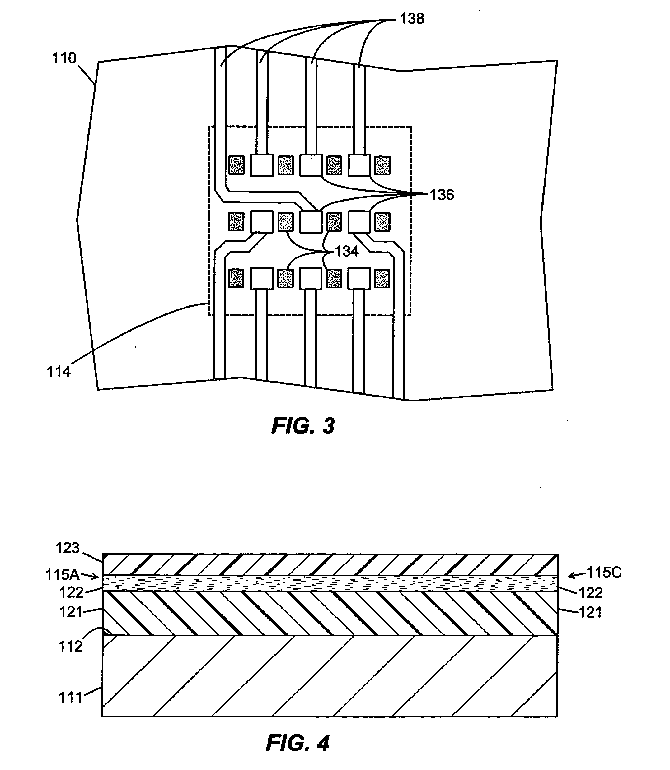
[0018] A first embodiment 100 of an optical apparatus according to the present invention is illustrated in FIGS. 1-3. A top plan view of optical apparatus 100 is shown inFIG. 1, a cross-sectional view is shown in FIG. 2, and second top plan view is shown in FIG. 3 with a component removed (as explained below). Referring to FIG. 1, Apparatus 100 comprises a main optical board 110 having a top surface, and an attachment area 114 located at the top surface for receiving an opto-electric component 210. Main optical board 110 comprises a plurality of optical waveguides 115A-115D, and opto-electric component 210 comprises a plurality of opto-electric devices 215A-215D. Each waveguide 115A-115D preferably has a microlens formed at its end, with the end being disposed adjacent to a side of attachment area 114 and facing opto-electric component 210. The microlenses of waveguides 115A and 115B serve to collimate or cross-collimate the waveguide's light beam into a light beam having a broader ...


PUM


Abstract

Disclosed are apparatuses and methods for fast and reliable integration of opto-electric components onto optical routing substrates. Accurate alignment of optical signals to and from the opto-electric components, and short electrical interconnect paths to the components to reduce signal delays to the devices on the components are enabled. In an exemplary embodiment, an attachment area is set out on the optical routing substrate to receive each component. One or more optical waveguides for coupling optical signals with the component are located adjacent to the attachment area. A plurality of conductive pads are located within the attachment area, and are for interconnecting to the component by way of bodies of solder, conductive adhesive, or the like. Interspersed between the conductive pads are a plurality of spacers that set a spacing distance between the attachment area and the opposing surface of the component, resulting in accurate alignment of optical signals.

Description

FIELD OF THE INVENTION [0001] The present invention relates to methods and apparatuses that integrate opto-electrical devices into optical pathways with precise optical alignment, and preferably with compact interconnections of electrical signals to the opto-electric devices. BACKGROUND OF THE INVENTION [0002] At present, the amount of information being transmitted through internet and high-speed data exchanges between servers is at a high level and growing rapidly. The information-technology (IT) industry is already encountering the physical limits of current electrical components, interconnections and assembly technologies. [0003] In making their invention, the inventors have recognized that optical devices could offer high speed data communication because the data signals stay within the optical layer throughout the entire routing path, without the need for expensive and complicated electrical-optical interfaces. However, that would require building complex optical communication ...

Claims


Application Information

Patent Timeline
Patent Type & Authority Applications(United States)
IPC IPC(8): G02B6/30
CPCG02B6/4232G02B6/305
Inventor LEE, MICHAEL G.YOKOUCHI, KISHIO
Owner FUJITSU LTD
Why Eureka
Try Eureka