Photovoltaic device

a photovoltaic and device technology, applied in the field of photovoltaic devices, can solve the problems of affecting the durability and reliability of the environment, affecting the grain boundaries of crystal grains with an increase in the size of crystal grains, etc., and achieves excellent barrier effect against alkalinity, prevent flux oozing and connection failure, and high reliability

Inactive Publication Date: 2006-03-30
SANYO ELECTRIC CO LTD
View PDF4 Cites 15 Cited by
  • Summary
  • Abstract
  • Description
  • Claims
  • Application Information

AI Technical Summary

Benefits of technology

[0014] In the above-mentioned invention, the arithmetic mean deviation (Ra) of the surface of the transparent conductive oxide film is 2 nm or less, a thickness of the silicon oxide insulation layer is approximately 1 to 10 times thicker than the arithmetic mean deviation (Ra) of the underlying transparent conductive oxide film, and the silicon oxide insulation film has the Si-2p peak with the full width at half maximum of 2.45 or less, which is evaluated by an X-ray photoelectron spectroscopy. Therefore the photovoltaic device has an excellent barrier effect against alkaline, and can obtain high reliability without reduction of adhesion between the collector electrode and transparent conductive oxide film.
[0015] The absence of the light-transmitting protective film at a joint part of the bus bar portions and the connecting tab prevent flux oozing and connection failure.

Problems solved by technology

However, because ITO films and ZnO films are polycrystals, their grain boundaries are affected with an increase in size of their crystal grains.
That is, the grain boundaries work as a path to accelerate alkaline to leach out from glass, thereby causing a possible decrease in the environment durability and reliability.

Method used


Image

  • Photovoltaic device
  • Photovoltaic device
  • Photovoltaic device

Examples


Embodiment Construction

)

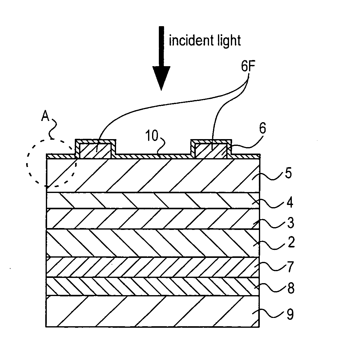
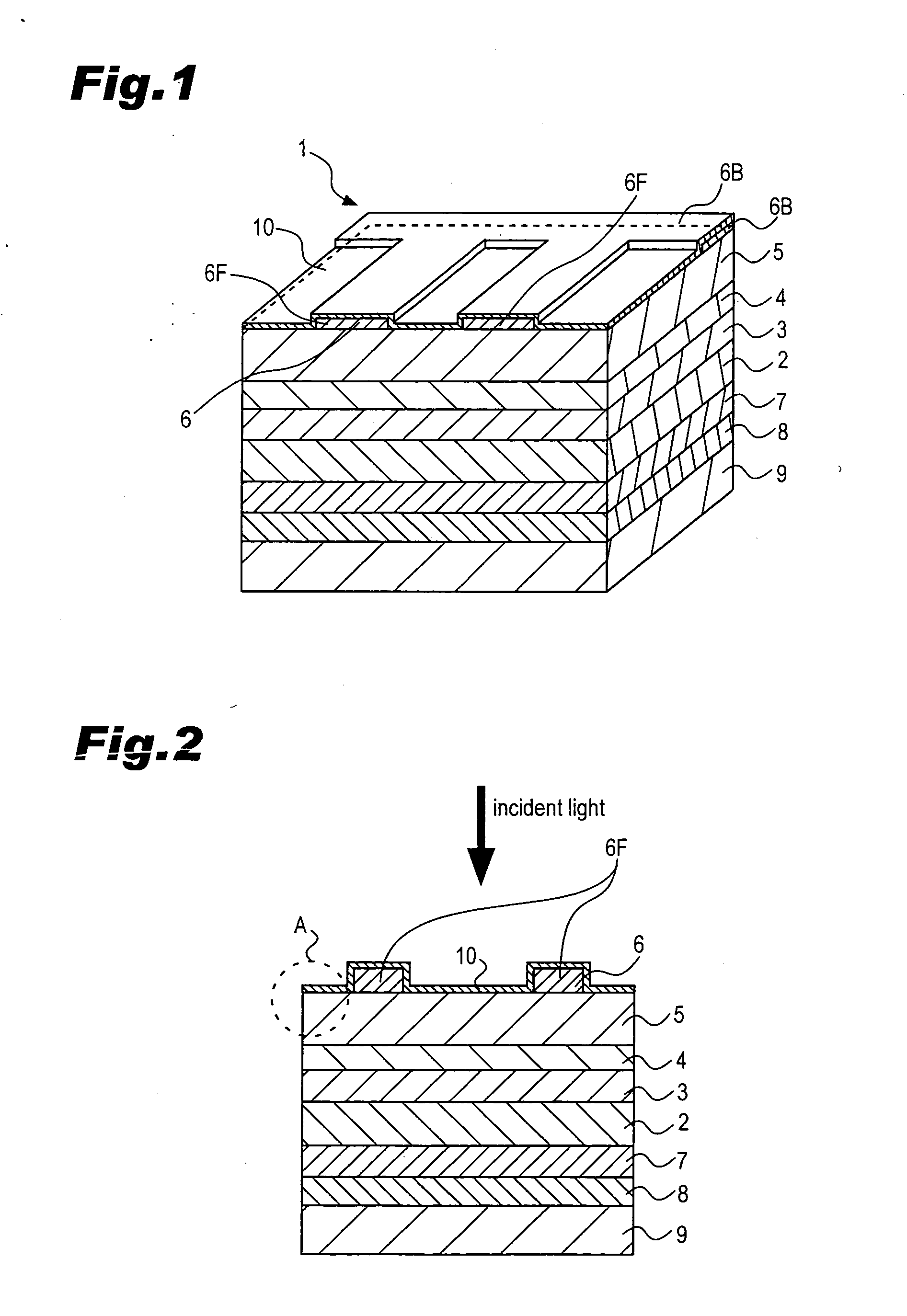
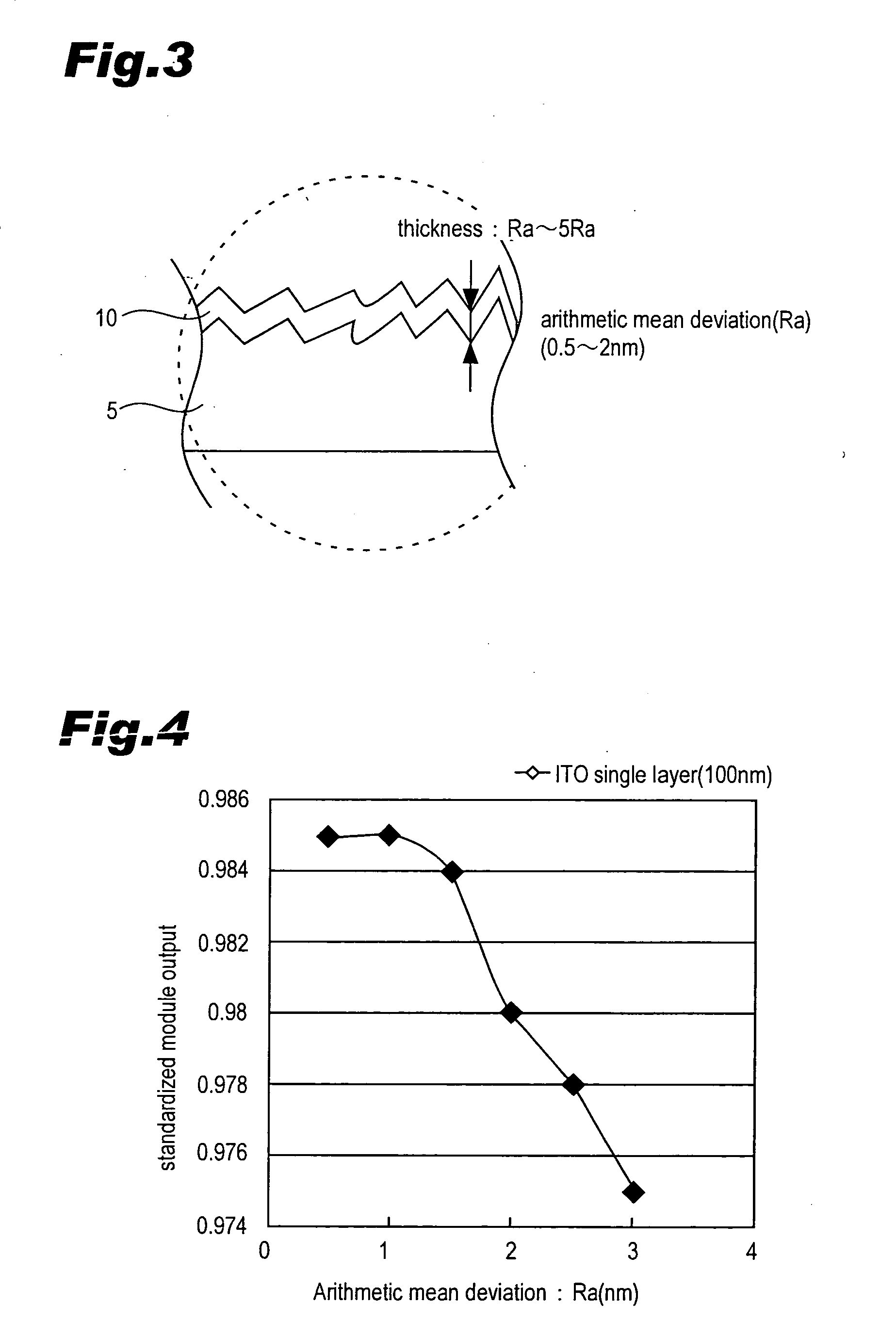
[0028] With reference to drawings, description will be made on an embodiment of the present invention below. FIG. 1 is a schematic perspective view showing a structure of a photoelectric conversion device according to the embodiment of the present invention. FIG. 2 is a schematic cross-sectional view showing the structure of the photoelectric conversion device according to the embodiment of the present invention.

[0029] The photoelectric conversion device 1 according to the embodiment, as shown in FIG. 1 and FIG. 2, comprises an n-type single crystal silicon substrate with a (100) plane 2 (hereinafter referred to as n-type single crystal silicon substrate 2) having resistivity of about 1 Ωcm, and a thickness of about 300 μm. There are pyramidal projections and depressions having a height of a few micro meters to a few tens of micro meters on a surface of the n-type single crystal silicon substrate 2. The projections and depressions are made for confining light. A substantially intr...


PUM

PropertyMeasurementUnit
Raaaaaaaaaaa
thicknessaaaaaaaaaa
Raaaaaaaaaaa

Abstract

The present invention provides a photovoltaic device having excellent environmental durability and good adhesion with a collector electrode made of metal paste. The photovoltaic device comprises an ITO film on a p-type amorphous silicon hydride film on a light incident side of the photovoltaic device and a collector electrode made of silver paste on the ITO film. A silicon oxide insulation film made of SiOx is provided on at least regions on the ITO film where the collector electrode is not formed. The thickness of the silicon oxide insulation film is about 1 to 10 times thicker than an arithmetic mean deviation (Ra) of the underlying ITO film. The silicon oxide insulation film is a film having a Si-2p peak with a full width at half maximum of 2.45 or less, which is evaluated by an X-ray photoelectron spectroscopy.

Description

[0001] The priority application Number 2004-283926 upon which this Patent application is based is hereby incorporated by reference. BACKGROUND OF THE INVENTION [0002] 1. Field of the Invention [0003] The present invention relates to a photovoltaic device, more particularly, to a photovoltaic device provided with a transparent conductive oxide film and a collector electrode on the transparent conductive oxide film and having greater environmental durability and reliability. [0004] 2. Description of the Related Art [0005] Since solar power generation systems mounted on a roof has become widespread rapidly, solar cells with greater environmental durability and environmental reliability than that of conventional home-use solar cells are required recently. Generally, the structures of solar cell modules are designed so as to obtain sufficient environmental durability, but more preferably, photoelectric conversion elements in the solar cell modules should possess excellent environmental d...

Claims


Application Information

Patent Timeline
Patent Type & Authority Applications(United States)
IPC IPC(8): H01L31/00H01L31/0216H01L31/04
CPCH01L31/022425H01L31/022466Y02E10/548H01L31/0747H01L31/077H01L31/03762H01L31/022475Y02E10/547
Inventor NAKASHIMA, TAKESHIMARUYAMA, EIJI
Owner SANYO ELECTRIC CO LTD
Why Eureka
Try Eureka