Semiconductor radiation detector and radiation detection apparatus

Inactive Publication Date: 2006-03-30
FUJIFILM HEALTHCARE CORP
View PDF7 Cites 0 Cited by
  • Summary
  • Abstract
  • Description
  • Claims
  • Application Information

AI Technical Summary

Benefits of technology

[0008] Since a single crystal of thallous bromide preferably containing 80.0 to 99.9 mol % of thallous bromide and 0.1 to 20.0 mol % of trivalent thallium (in terms of tribromobis thallium) is used, resistivity is made uniform in a wide area inside the single crystal, lattice defects are further reduced and energy resolution and sensitivity of the semiconductor radiation detector are furthe

Problems solved by technology

Based on this verification, the present inventors discovered that this semiconductor radiation

Method used


Image

  • Semiconductor radiation detector and radiation detection apparatus
  • Semiconductor radiation detector and radiation detection apparatus
  • Semiconductor radiation detector and radiation detection apparatus

Examples


Embodiment Construction

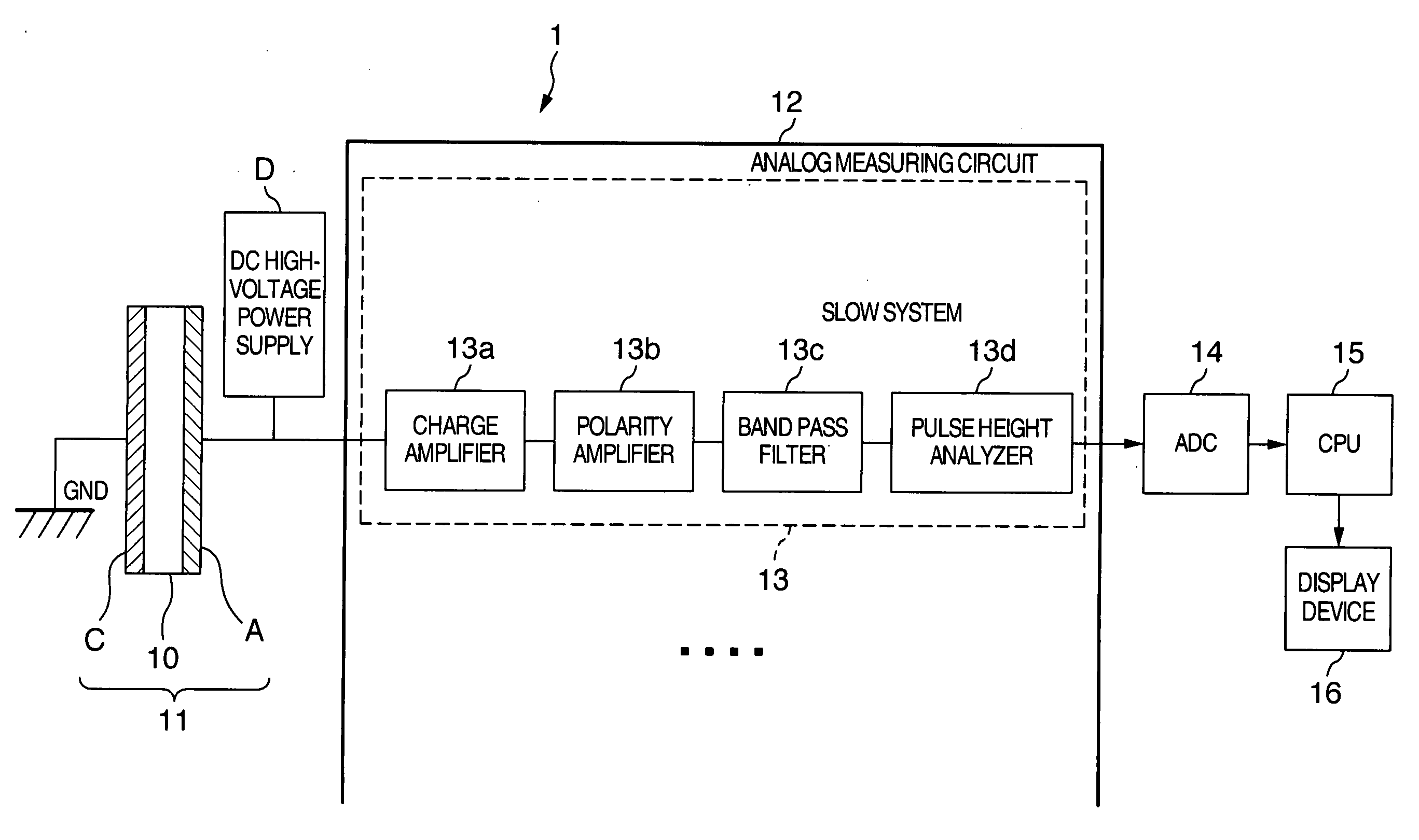
[0017] A radiation detection apparatus which is an embodiment of the present invention will be explained in detail using FIG. 1. The radiation detection apparatus 1 of the present embodiment is an apparatus for detecting radiation such as X-rays and γ-rays, and detection of γ-rays will be explained as an example here. The radiation detection apparatus 1 is provided with a semiconductor radiation detector 11, an analog measuring circuit 12, an analog / digital converter (hereinafter referred to as “ADC”) 14 and a central processing unit (hereinafter simply referred to as “CPU”) 15. Reference character D denotes a DC high-voltage power supply. The analog measuring circuit 12 can also be constructed of an ASIC (application-specific integrated circuit).

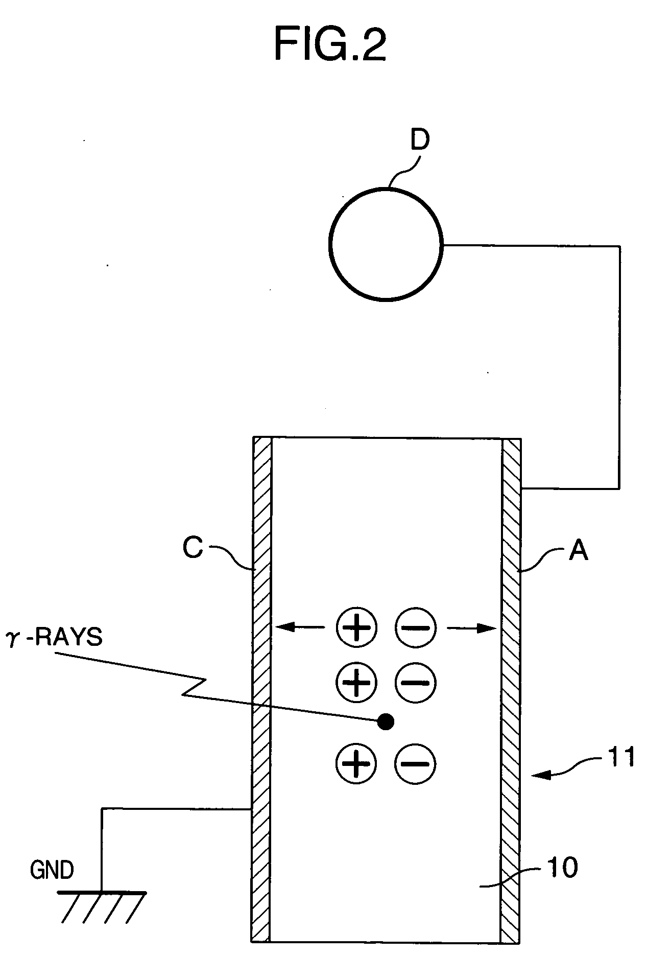
[0018] The semiconductor radiation detector 11 is provided with a semiconductor radiation detection element (hereinafter referred to as “semiconductor detection element”) 10 and a cathode electrode C and an anode electrode A attached to th...


PUM


Abstract

The present invention provides a semiconductor radiation detector and radiation detection apparatus capable of improving energy resolution and the semiconductor radiation detection apparatus includes a semiconductor radiation detector and a signal processing circuit which processes a radiation detection signal output from the semiconductor radiation detector. The semiconductor radiation detector is provided with anode electrodes A and cathode electrodes C disposed so as to face each other with semiconductor radiation detection elements placed in-between. The semiconductor radiation detection element is made up of a single crystal of thallous bromide containing trivalent thallium (e.g., tribromobis thallium). The semiconductor radiation detector containing such a semiconductor radiation detection element reduces lattice defects in the single crystal and thereby increases charge collection efficiency.

Description

BACKGROUND OF THE INVENTION [0001] The present invention relates to a semiconductor radiation detector and radiation detection apparatus. [0002] Conventionally, an X-ray machine or radiological imaging apparatus uses a semiconductor radiation detector for detecting radiation such as X-rays which pass through an examinee and γ-rays emitted from a radioactive material given to an examinee. As such a semiconductor radiation detector, one using a semiconductor radiation detection element made of a single crystal of cadmium telluride (CdTe) is known (e.g., see JP-A-2002-168958 (paragraph 0025 and paragraph 0027)). With this semiconductor radiation detector, an attempt is made to increase detection sensitivity of radiation using a single crystal of cadmium telluride with a small content of impurities. Furthermore, JP-A-2002-168958 (paragraph 0025 and paragraph 0027) also describes a semiconductor radiation detection element composed of a polycrystal of thallous bromide (TlBr). [0003] The ...

Claims


Application Information

Patent Timeline
IPC IPC(8): G01T1/24H01L27/14H01L31/09
CPCG01T1/24
Inventor KITAGUCHI, HIROSHIAMEMIYA, KENSUKEYOKOI, KAZUMAUENO, YUUICHIROUTSUCHIYA, KATSUTOSHIYANAGITA, NORIHITOKOJIMA, SHINICHIHITOMI, KEITAROSHOJI, TADAYOSHI
Owner FUJIFILM HEALTHCARE CORP
Why Eureka
Try Eureka